


ZC706 Evaluation Board User Guide
43
UG954 (v1.5) September 10, 2015
Feature Descriptions
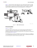
lists the GTX Bank interface connections between the AP SoC U1 and FMC LPC
connector J5.
For additional information on Zynq-7000 GTX transceivers, see
7 Series FPGAs GTX/GTH
Transceivers User Guide
(
).
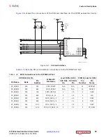
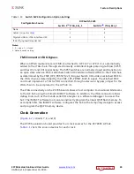
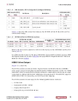
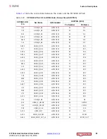
Table 1-15:
AP SoC GTX Bank 111 Interface Connections to FMC LPC J5
Transceiver
Bank
AP SoC U1
Pin
Number
AP SoC U1 Pin
Name
Schematic Net Name
Connected
Pin
Connected
Device
GTX_BANK_11
1
AB2
MGTPTXP0_111
FMC_LPC_DP0_C2M_P
C2
FMC LPC
J5
AB1
MGTPTXN0_111
FMC_LPC_DP0_C2M_N
C3
AC4
MGTPRXP0_111
FMC_LPC_DP0_M2C_P
C6
AC3
MGTPRXN0_111
FMC_LPC_DP0_M2C_N
C7
Y2
MGTPTXP1_111
SMA_MGT_TX_P
J35.1
GTX TX/RX
SMA
Y1
MGTPTXN1_111
SMA_MGT_TX_N
J34.1
AB6
MGTPRXP1_111
SMA_MGT_RX_P
J32.1
AB5
MGTPRXN1_111
SMA_MGT_RX_N
J33.1
W4
MGTPTXP2_111
SFP_TX_P
18
SFP+
Conn. P2
W3
MGTPTXN2_111
SFP_TX_N
19
Y6
MGTPRXP2_111
SFP_RX_P
13
Y5
MGTPRXN2_111
SFP_RX_N
12
V2
MGTPTXP3_111
(capacitively coupled to AA4)
U1.AA4
AP SoC U1
GTX
Loopback
V1
MGTPTXN3_111
(Cooperatively coupled to AA3)
U1.AA3
AA4
MGTPRXP3_111
See Pin V2 loopback
U1.V2
AA3
MGTPRXN3_111
See Pin V1 loopback
U1.V1
U8
MGTREFCLK0P_111
FMC_LPC_GBTCLK0_M2C_C_P
D4
FMC LPC
J5
U7
MGTREFCLK0N_111
FMC_LPC_GBTCLK0_M2C_C_N
D5
W8
MGTREFCLK1P_111
SMA_MGT_REFCLK_P
J36.1
GTX
REFCLK
SMA
W7
MGTREFCLK1N_111
SMA_MGT_REFCLK_N
J31.1
Notes:
1. AP SoC U1 GTX input clock nets are capacitively coupled to the FMC LPC J5 pins.
2. AP SoC U1 GTX input nets are capacitively coupled to the RX and MGT_REFCLK SMA pins.


