


ZC706 Evaluation Board User Guide
64
UG954 (v1.5) September 10, 2015
Feature Descriptions
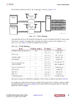
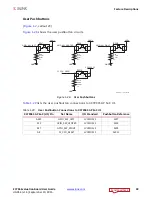
shows SW10.
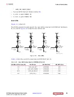
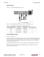
PS Power-On and System Reset Pushbuttons
shows the reset circuitry for the processing system.
Depressing and then releasing pushbutton SW1 causes PS_POR_B_SW to strobe low.
PS_POR_B:
This reset is used to hold the PS in reset until all PS power supplies are at the
required voltage levels. It must be held Low through PS power-up. PS_POR_B should be
generated by the power supply
power-good
signal.
X-Ref Target - Figure 1-31
Figure 1-31:
PROG_B Pushbutton SW10
UG954_c1_31_041113
FPGA_PROG B
VCC3V3
R73
4.7 k
Ω
0.1 W
5%
GND
2
1
3
4
SW10
X-Ref Target - Figure 1-32
Figure 1-32:
PS Power On and System Reset Circuitry
UG954_c1_32_041113
MAX16025
Dual Voltage Monitor
and Sequencer
2
3
6
13
9
4
U8
7
8
TH1
12
11
10
15
17
14
16
5
TH0
TOL
MR_B
EN2
EN1
IN2
IN1
GND
EPAD
CRESET
CDLY2
CDLY1
OUT2
OUT1
RST_B
1
VCC
VCCP1V8
R177
8.06 K
Ω
0.1W
1%
R264
10.0
Ω
0.1W
1%
VCCP1V8
R265
10.0 K
Ω
0.1W
1%
R149
249
Ω
0.1W
1%
R176
8.06 K
Ω
0.1W
1%
R256
10.0 K
Ω
0.1W
1%
R263
10.0 K
Ω
0.1W
1%
R262
10.0 K
Ω
0.1W
1%
R261
10.0 K
0.1W
1%
J7
1
2
SW3
1
2
SW2
GND
VCCP1V8
PS_POR_B
PS_SRST_B
C8
DNP
DNP
xxx
C7
0.1 µf
25V
X5R
C6
270pF
25V
X5R
GND
VCC3V3_PS
DS1
GND
PS_POR_B_SW
PS_SRST_B_SW
1
2
3
J44
VCCP1V8
R266
10.0 K
Ω
0.1W
1%
1
2
3
J43
PS_POR_B
PS_SRST_B
VCC3V3
C8 = DNP, SRST delay = 35 µS
C6 = 270 pF, POR delay = 1.08 mS


