


ZC706 Evaluation Board User Guide
24
UG954 (v1.5) September 10, 2015
Feature Descriptions
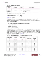
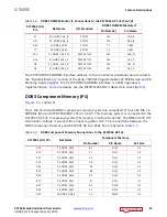
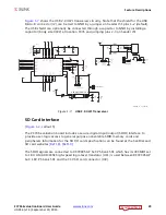
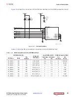
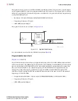
The ZC706 DDR3 component interface adheres to the constraints guidelines documented in
the
DDR3 Design Guidelines
section of
Zynq-7000 All Programmable SoC PCB Design and
Pin Planning Guide
(
). The ZC706 DDR3 component interface is a 40
Ω
impedance
implementation. For more details, see the MT41J256M8HX-15E data sheet
.
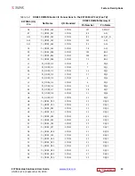
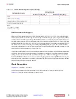
L27
PS_DDR3_A2
L3
A2
U2, U3, U4, U5
G25
PS_DDR3_A3
K2
A3
U2, U3, U4, U5
J26
PS_DDR3_A4
L8
A4
U2, U3, U4, U5
G24
PS_DDR3_A5
L2
A5
U2, U3, U4, U5
H26
PS_DDR3_A6
M8
A6
U2, U3, U4, U5
K22
PS_DDR3_A7
M2
A7
U2, U3, U4, U5
F27
PS_DDR3_A8
N8
A8
U2, U3, U4, U5
J23
PS_DDR3_A9
M3
A9
U2, U3, U4, U5
G26
PS_DDR3_A10
H7
A10
U2, U3, U4, U5
H24
PS_DDR3_A11
M7
A11
U2, U3, U4, U5
K23
PS_DDR3_A12
K7
A12
U2, U3, U4, U5
H23
PS_DDR3_A13
N3
A13
U2, U3, U4, U5
J24
PS_DDR3_A14
N7
A14
U2, U3, U4, U5
M27
PS_DDR3_BA0
J2
BA0
U2, U3, U4, U5
M26
PS_DDR3_BA1
K8
BA1
U2, U3, U4, U5
M25
PS_DDR3_BA2
J3
BA2
U2, U3, U4, U5
K25
PS_DDR3_CLK_P
F7
CK
U2, U3, U4, U5
J25
PS_DDR3_CLK_N
G7
CK_B
U2, U3, U4, U5
M22
PS_DDR3_CKE
G9
CKE
U2, U3, U4, U5
N23
PS_DDR3_WE_B
H3
WE_B
U2, U3, U4, U5
M24
PS_DDR3_CAS_B
G3
CAS_B
U2, U3, U4, U5
N24
PS_DDR3_RAS_B
F3
RAS_B
U2, U3, U4, U5
F25
PS_DDR3_RESET_B
N2
RESET_B
U2, U3, U4, U5
N22
PS_DDR3_CS_B
H2
CS_B
U2, U3, U4, U5
L23
PS_DDR3_ODT
G1
ODT
U2, U3, U4, U5
N21
PS_VRN
M21
PS_VRP
L22
VTTVREF_PS
L24
VTTVREF_PS
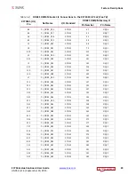
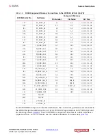
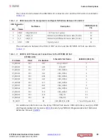
Table 1-5:
DDR3 Component Memory Connections to the XC7Z045 AP SoC
(Cont’d)
XC7Z045 (U1) Pin
Net Name
Component Memory
Pin Number
Pin Name
Ref. Des.


