


Manual BG41/BG42/BG43
Interface modules
Rev. 99/49
3-53
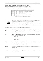
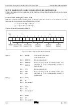
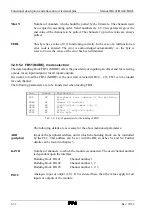
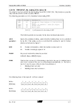
MODE
Bit number
0
= 0 signed
1 unsigned
1
= 0 binary representation from Wandler -2048...2047
(0...4095)
1 normalised representation in mV or mA
2
= 0 no bottom limit for current measurement
1 bottom limit 4 mA
OFFS
Offset to the zero point of the input/output
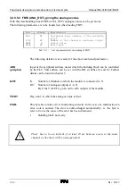
FEHL
This byte has a value of 0, if functioning correctly. In the case of a malfunction an
error code is entered. The error is acknowledged automatically, i.e. the byte is
reset to 0 once the cause of the error has been eliminated.
1
Building block not ready
2
Building block does not answer
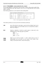
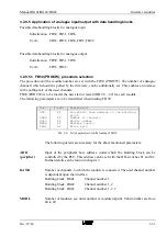
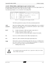
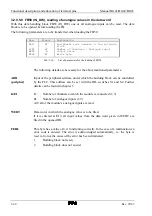
3.2.9.5.3 FB52 (ANA_IN), reading of analogue value
With this data handling block FB52 (ANA_IN) an analogue input can be read.
The following paramters are to be transferred when loading FB52:
Des.
Format
Explanation
ADR
KF
Peripheral base address of the building
block
K/EI
KY
Number of channels / analogue input
WERT
W
Output value
FEHL
BY
Error byte
Tab. 3-10:
List of parameters for the loading of FB52
The following details are necessary for the abovementioned parameters:
ADR
(peripher)
Input of the peripheral address, under which the building block can be controlled
by the PLC. This address can be set with the DIL switches S1 and S2. Further
details can be found in chapter 5.
K/EI
K:
Number of channels to which the module is connected (1-3).
EI:
Number of analogue inputs (1-8)
WERT
Flag word, in which the analogue value is filed.
FEHL
This byte has a value of 0, if functioning correctly. In the case of a malfunction an
error code is entered. The error is acknowledged automatically, i.e. the byte is
reset to 0 once the cause of the error has been eliminated.
1
Building block not ready
2
Building block does not answer
Summary of Contents for SSM-BG41
Page 2: ...Lerrzeichen...
Page 8: ...Contents Manual BG41 BG42 BG43 iv Rev 99 49...
Page 10: ......
Page 16: ......
Page 26: ...Firmware s memory distribution Manual BG41 BG42 BG43 2 10 Rev 99 49...
Page 28: ......
Page 53: ...Manual BG41 BG42 BG43 Interface modules Rev 99 49 3 25 3 2 7 2 Data flow Fig 3 26 Data flow...
Page 114: ...Functional description and allocation of terminal pins Manual BG41 BG42 BG43 3 86 Rev 99 49...
Page 116: ......
Page 215: ...Manual BG41 BG42 BG43 Software Rev 99 49 4 99 Month 06h Year 95h Weekday Tuesday 02h...
Page 222: ...Application of interfaces without data handling blocks Manual BG41 BG42 BG43 4 106 Rev 99 49...
Page 224: ......
Page 258: ...Structure guidelines Manual BG41 BG42 BG43 5 34 Rev 99 49...
Page 260: ......
Page 274: ...Overview cycle load Manual BG41 BG42 BG43 6 14 Rev 99 49...
Page 275: ...Appendix A List of figures A 1 B Index of tables B 1 C Index C 1...
Page 276: ......
Page 280: ...List of figures Manual BG41 BG42 BG43 A 4 Rev 99 49...


