


Application of interfaces without data handling blocks
Manual BG41/BG42/BG43
4-86
Rev. 99/49
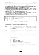
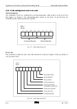
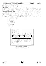
BIT 5 = 1:
indicates, that the building block has received data, which is to be found in the reception buffer. If
the corresponding channel also functions as the receiver, this bit should be cyclically polled, so that
the data can be read where necessary. Otherwise an overflow can occur in the reception buffer.
If bit 5 = 0, reading access is not allowed, as in this case the building block does not acknowledge
this. It also takes 20 µs before another character is made available in the reception channel.
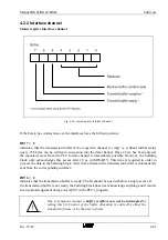
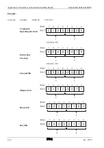
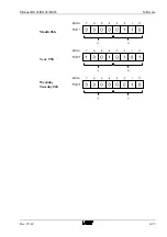
Data register interface channel
If a channel is used for the operation of a DCF77 antenna module, information on the DCF77
system can be read on a continuous basis.
The bits of the corresponding periphery bytes have the following significance:
Fig. 4-15: Data register interface channel
Summary of Contents for SSM-BG41
Page 2: ...Lerrzeichen...
Page 8: ...Contents Manual BG41 BG42 BG43 iv Rev 99 49...
Page 10: ......
Page 16: ......
Page 26: ...Firmware s memory distribution Manual BG41 BG42 BG43 2 10 Rev 99 49...
Page 28: ......
Page 53: ...Manual BG41 BG42 BG43 Interface modules Rev 99 49 3 25 3 2 7 2 Data flow Fig 3 26 Data flow...
Page 114: ...Functional description and allocation of terminal pins Manual BG41 BG42 BG43 3 86 Rev 99 49...
Page 116: ......
Page 215: ...Manual BG41 BG42 BG43 Software Rev 99 49 4 99 Month 06h Year 95h Weekday Tuesday 02h...
Page 222: ...Application of interfaces without data handling blocks Manual BG41 BG42 BG43 4 106 Rev 99 49...
Page 224: ......
Page 258: ...Structure guidelines Manual BG41 BG42 BG43 5 34 Rev 99 49...
Page 260: ......
Page 274: ...Overview cycle load Manual BG41 BG42 BG43 6 14 Rev 99 49...
Page 275: ...Appendix A List of figures A 1 B Index of tables B 1 C Index C 1...
Page 276: ......
Page 280: ...List of figures Manual BG41 BG42 BG43 A 4 Rev 99 49...


