


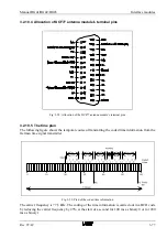


Functional description and allocation of terminal pins
Manual BG41/BG42/BG43
3-82
Rev. 99/49
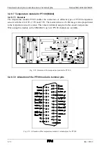
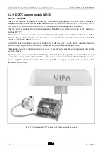
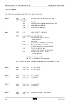
3.2.10.13 Application of the DCF77 antenna module with data handling blocks
Possible data handling blocks
Initialization FB100, FB101
Cycle
FB102
The DCF77 antenna module consists of a DCF77 reception unit, which provides a 20mA current
loop interface with the received decode time signal. One needs a 20mA current loop module for the
transmission of the time signal. The function blocks FB100 or FB101 and FB5 are required for the
application of an antenna module. From the firmware 4118V12 the transmission parameters are
automatically set when the DCF77 function is selected, as long as the jumper J11 is plugged into
position 75 to 19200 (FB5 not required). The synchronisation of the clock situated on the building
block is carried out by the firmware every full hour. See chapter 4.1.3.2 for details on the operation
of the clock on the interface building block.
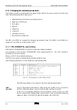
The parameters for the data handling blocks are explained in the following chapters:
FB100 see chapter 4.1.4.1
FB5
see chapter 4.1.3.1
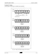
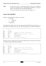
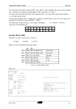
Example:
The following example shows how an interface building block is to be parametrized, so that one can
read the time signal of a DCF77 antenna module with a 20mA current loop module.
FB100 (PROCW)
Channel 1 of the building block should be set for the operation of the antenna module. The building
block’s base address is F0A0. Any error which may arise should be filed in the flag byte MB127.
SPA FB100
NAME
:PROCW
ADR
:KH F0A0
Building block’s absolute base address
KANR
:KF+1
Channel 1
PROC
:KF+7
Code for DCF77 antenna module
FEHL
:MB127
Error code in flag byte 127
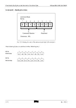
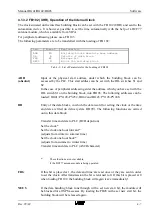
FB5 (PARAMETR)
In this example the building block’s DIL switches are to be set to the absolute address F0A0h. The
plug connector J11 is in the position 150-38400baud. Any error code which may arise is to be filed
in MB127. Channel 1is to be set to the following values:
4800baud, 8bit/character, 1 stop bit, with even parity
SPA FB5
NAME
:PARAMETER
ADR
:KH F0A0
Building block’s absolute base address
K/0
:KY1,0
Channel
BAUD
:KF+8
Baud rate = 4800 (according to the table)
ZEI
:KF+8
8 bit/character
PARI
:KY1,1
with parity, even parity
STOP
:KF+1
1 Stop bit
FEHL
:MB127
Error code in flag byte 127
Summary of Contents for SSM-BG41
Page 2: ...Lerrzeichen...
Page 8: ...Contents Manual BG41 BG42 BG43 iv Rev 99 49...
Page 10: ......
Page 16: ......
Page 26: ...Firmware s memory distribution Manual BG41 BG42 BG43 2 10 Rev 99 49...
Page 28: ......
Page 53: ...Manual BG41 BG42 BG43 Interface modules Rev 99 49 3 25 3 2 7 2 Data flow Fig 3 26 Data flow...
Page 114: ...Functional description and allocation of terminal pins Manual BG41 BG42 BG43 3 86 Rev 99 49...
Page 116: ......
Page 215: ...Manual BG41 BG42 BG43 Software Rev 99 49 4 99 Month 06h Year 95h Weekday Tuesday 02h...
Page 222: ...Application of interfaces without data handling blocks Manual BG41 BG42 BG43 4 106 Rev 99 49...
Page 224: ......
Page 258: ...Structure guidelines Manual BG41 BG42 BG43 5 34 Rev 99 49...
Page 260: ......
Page 274: ...Overview cycle load Manual BG41 BG42 BG43 6 14 Rev 99 49...
Page 275: ...Appendix A List of figures A 1 B Index of tables B 1 C Index C 1...
Page 276: ......
Page 280: ...List of figures Manual BG41 BG42 BG43 A 4 Rev 99 49...


