background image

5-10

5.4 Removing the LCD Module and FL

Inverter Board

1.

Remove the battery pack as indicated in Section 5.2.

2.

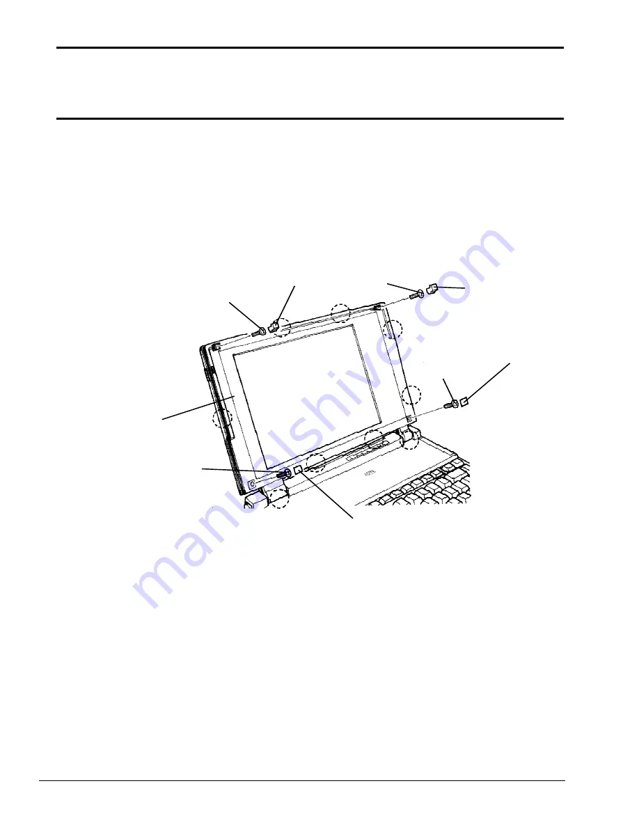
Open the display panel.  Then remove the two rubber cushions and the two plastic seals
from the LCD mask.  Then lay the LCD module back on the LCD support block to support
the LCD module.

3.

Remove the four (M2x4) screws securing the LCD mask.  Then move the LCD module to
its upright position.

Figure 5-5  Removing the LCD rubber cushions, plastic seals, and screws

plastic
seal

LCD mask

M2x4
screw

rubber cushion

M2x4 screw

M2x4
screw

plastic seal

M2x4
screw

rubber cushion

Summary of Contents for T-Series T2200sx

Page 1: ...1 1 Chapter 1 Hardware Overview ...

Page 2: ...1 2 This page intentionally left blank ...

Page 3: ... Board 1 15 Tables Table 1 1 3 5 inch FDD specifications 1 11 Table 1 2 2 5 inch HDD specifications 1 12 Table 1 3 Sidelit LCD specifications 1 14 Table 1 4 FL inverter board specifications 1 15 Figures Figure 1 1 T2200SX personal computer 1 7 Figure 1 2 T2200SX system unit configuration 1 7 Figure 1 3 T2200SX block diagram 1 8 Figure 1 4 3 5 inch FDD 1 11 Figure 1 5 2 5 inch HDD 1 12 Figure 1 6 K...

Page 4: ...1 4 This page intentionally left blank ...

Page 5: ...patible with the Lotus Intel Microsoft Expanded Memory Specification LIM EMS The standard memory is expandable by 2 4 or 8MB increments to a maximum of 10MB Disk Storage An internal 2 5 40MB 60MB or 80MB Hard Disk Drive HDD provides an average access time of 19ms A 3 5 Floppy Disk Drive FDD supports 2HD 1 44MB as well as 2DD 720KB Display A new larger surface area high resolution fully adjustable ...

Page 6: ...ch keeps the date and time and system configuration even when power is off Mouse Port A PS 2 mouse connector is located on the right side of the computer Interface Ports A parallel port serial port RGB port numeric keypad port and expansion bus connector are provided to allow the T2200SX to interface with a variety of optional equipment ...

Page 7: ...1 7 The T2200SX Personal Computer is shown in Figure 1 1 and the T2200SX system configuration is shown in Figure 1 2 Figure 1 1 T2200SX personal computer Figure 1 2 T2200SX system unit configuration ...

Page 8: ...1 8 1 2 System Unit Block Diagram Figure 1 3 is a block diagram of the T2200SX system unit Figure 1 3 T2200SX block diagram ...

Page 9: ...er FDC TC8565 One Serial Input Output Controller SIO TC8570 One Variable Frequency Oscillator VFO TC8568 One I O Controller Real Time Clock RTC 146818AF The RTC chip stores the date time and system configuration with power supplied from the RTC battery Keyboard Controller KBC U37452 Power Supply Controller PSC U47C440 Memory Standard RAM 2MB Backup RAM 32KB BIOS ROM 128KB 96KB are used BIOS ROM co...

Page 10: ...X2 28 322MHz OSC X3 and 25 175MHz OSC X4 are used for the video 14 7456MHz OSC X5 is used for the COM 14 31818MHz OSC X6 is used for the KBC 32 768KHz OSC X7 is used for the RTC 24MHz OSC X8 is used for the FDC and VFO See Appendix A for the location of the oscillators ...

Page 11: ...ations are described in Table 1 1 Figure 1 4 3 5 inch FDD Table 1 1 3 5 inch FDD specifications Item 2 Mbyte mode 1 Mbyte mode Storage capacity Kbyte Unformatted Formatted 2 000 1 440 1 000 720 Number of heads 2 2 Number of cylinders 80 80 Access time ms Track to track Average Head settling time 3 94 15 3 94 15 Recording track density tpi 135 135 Data transfer rate Kbps 500 250 Rotation speed rpm ...

Page 12: ...ength Limited UPDATE Item 40MB 60MB 80MB CP 2044 JD E2850P CP 2064 JD E2085M Storagecapacity Formatted Mbytes 42 5 42 52 64 0 85 68 Numberofdisks 2 2 2 2 Dataheads 4 3 4 4 Datasurfaces 4 3 4 4 Trackspersurface 552 791 2 823 791 2 Tracksperdrive 2 208 2 373 6 1 306 3 164 Sectorspertrack 38 1 35 1 38 1 35 1 Bytespersector 512 512 512 512 Accesstime ms Tracktotrack Average Maximum 5 19 40 9 25 47 5 1...

Page 13: ...eyboard is mounted in the system unit The keyboard is connected to the keyboard controller located on the system board through a 19 pin flat cable The keyboard is shown in Figure 1 6 See Appendix E for optional keyboard configurations Figure 1 6 Keyboard ...

Page 14: ...LCD receives vertical and horizontal synchronizing signals 8 bit data signals 4 bit upper data signal 4 bit lower data signal and shift clock for data transmission from the PVGA1F video controller All signals are CMOS level compatible The sidelit LCD is shown in Figure 1 7 and its specifications are described in Table 1 3 Figure 1 7 Sidelit LCD Table 1 3 Sidelit LCD specifications Item Specificati...

Page 15: ...Min Current mA 5 5 Frequency KHz 39 Bounds of current mA 3 25 5 5 1 6 2 FL Inverter Board The FL inverter board supplies the high frequency current needed to illuminate the FL The specifications for the FL inverter board are described in Table 1 4 Table 1 4 FL inverter board specifications ...

Page 16: ...1 16 This page intentionally left blank ...

Page 17: ...2 1 Chapter 2 Operational Overview ...

Page 18: ...2 2 This page intentionally left blank ...

Page 19: ...Printer Port 2 20 2 11 Keyboard Controller 2 21 2 11 1 Key Code Generation 2 21 2 11 2 Mouse Control Command 2 22 2 12 RS 232 C Port 2 24 2 12 1 Data Format 2 24 2 12 2 Input Output Port 2 25 2 12 3 25 pin Connector 2 25 2 13 Connectors 2 26 Tables Table 2 1 Interrupt assignment 2 13 Table 2 2 NMI 2 14 Table 2 3 DMA channel assignment 2 15 Table 2 4 PIT channel usage 2 16 Table 2 5 PIT I O ports 2...

Page 20: ...4 Figures Figure 2 1 System unit block diagram 2 6 Figure 2 2 Real Mode Memory Map 2 9 Figure 2 3 Protected Mode Memory Map 2 10 Figure 2 4 DRAM address map 2 12 Figure 2 5 Start parity and stop bits 2 24 ...

Page 21: ... video RAM Optional memory Maximum 8MB for a system total of 10MB One expansion memory slot is available for 2 4 or 8MB memory cards No parity bit Access time 70ns T9901 Super Integrations SI This Super Integration SI includes the following components Two Direct Memory Access Controllers DMACs 82C37A Two Programmable Interrupt Controllers PICs 82C59A One Programmable Interval Timer PIT 82C54 One F...

Page 22: ... block diagram CPU 80386SX SYSCNT GA MEMCNT BUSCNT BUSDRV ADRDRV NDP 80387SX RTC Main Memory BIOS ROM SI9901 DMAC 80C37 x2 PIC 80C59 x2 TIM 80C54 x1 FDC TC8565 x1 UART TC8570 x1 VFO TC8568 x1 IOCNTx1 Speaker LCD 640x480 Display Controller 3 5 inch FDD RS 232 C DRV RGB Port COMMS Port VRAM 256KB 2 5 inch HDD HDC Expansion Connector 150 pin KBC Ten key Port Mouse Port Option Keyboard Built in Option...

Page 23: ... of protection and an optional paging mechanism For the details about the 80386SX hardware and its instruction set refer to the Intel 80386SX Hardware Reference Manual and Programmer s Reference Manual 2 2 1 Clock Mode The 80386SX processor can operate at clock rates of 20MHz high speed and 10 MHz low speed To switch between the two rates hold down the Fn key and press the PgDn key to select slow ...

Page 24: ...are Refer to the MS DOS Manual for details about how to use extended and expanded memory The extended memory can be increased by an optional 2MB 4MB or 8MB to a system total of 10MB The RAM above 640KB and below 1MB is extra memory and it can be mapped to the 100000 address as extended memory The 640KB BIOS ROM contains the system BIOS VGA BIOS and IRT The ROM data bus width is 8 bits The system B...

Page 25: ...re 2 2 Real Mode Memory Map Conventional Memory 640 KB Video RAM for VGA 128 KB VGA BIOS ROM 32 KB Reserved Hard RAM Window 32 KB Back up RAM 32 KB System BIOS ROM 64 KB CPU ADDRESS 000000 0A0000 0C0000 0C8000 0E0000 0E8000 0F0000 100000 ...

Page 26: ...8000 0F0000 100000 260000 300000 500000 900000 F00000 FF0000 FFFFFF Back up RAM 32KB System BIOS ROM 64KB Extended Memory 1408KB Optional Memory Card 2MB Optional Memory Card 4MB Optional Memory Card 8MB Compatible Bus System BIOS ROM 64KB Hard RAM Window 32KB Reserved VGA BIOS ROM 32KB Video RAM for VGA 128KB Conventional Memory 640KB ...

Page 27: ...y The Extended Memory DRAM start address base address is assigned beyond the conventional memory size and Hard RAM size Using a special register extended memory is set in 64KB incre ments except for the conventional memory and Hard RAM which are used for extended memory 2 3 5 Hard RAM Hard RAM is accessed through the 32KB Hard RAM window Hard RAM is assigned from address 0E0000 to 0E7FFF Hard RAM ...

Page 28: ...DRAM address map Memory address map 000000 0A0000 0C0000 0C8000 0E0000 0E8000 0F0000 0FFFFF DRAM address map 000000 0A0000 0B0000 0C0000 Conventional Memory 640KB Conventional Memory 640KB Video BIOS 32KB System BIOS 64KB Video RAM 128KB Video BIOS 32KB Reserved H RAM Extended Memory H RAM Window 32KB System BIOS 64KB Back up RAM 32KB ...

Page 29: ...n interrupt request from the intelligent power supply is detected The math co processor 80387SX generates an INT 13 interrupt by itself and its interrupt handler executes INT 02 that is an NMI interrupt vector Interrupt Level Assigned to NMI RAM Parity Error I O Channel Error 1 0 Timer 1 Keyboard 2 PIC 2 for level 8 to 15 3 Secondary Communications COM 2 4 Primary Communications COM 1 5 PRT 2 6 FD...

Page 30: ...The bit assignment of this register is as follows Bit 7 Mask A 0 enables the register to generate the NMI signal which is then sent to the Central Processor while 1 disables the NMI signal This bit will be set to 1 at system power on Bits 6 0 Reserved 2 4 2 PIC There are two 82C59A equivalent Programmable Interrupt Controllers PICs contained in the SI T9901 to handle 15 levels of maskable interrup...

Page 31: ...C 1 contains channels 0 through 3 These channels transfer data as bytes 8 bits between the I Os and the T2200SX working memory in 64KB blocks DMAC 2 contains channels 4 through 7 Channel 4 is used to cascade channels 0 through 3 to the Central Processor Channels 5 through 7 transfer data as words 16 bits between the I Os and working memory in 128KB blocks Channels 5 through 7 cannot transfer data ...

Page 32: ... The time of day channel periodically generates the level 0 interrupt request to the central processor The usage and I O port assignments for the PIT are presented in Table 2 4 and Table 2 5 Table 2 4 PIT channel usage Table 2 5 PIT I O ports Channel Use 0 System Timer 1 Dynamic RAM Refresh Request 2 Audio Signal for Speaker Port I O Description 040 I O Channel 0 Count Register 041 I O Channel 1 C...

Page 33: ...m sets 1 to 1 in the T2GT bit of the System Command to generate the audio signal Number 2 is set to 1 in the SPKD bit of the System Command Register which sends the audio signal to the Speaker By reading the System Status and checking the TC2O bit the program can determine whether the PIT device in channel 2 generates an audio signal ...

Page 34: ... battery is used for RTC back up power 50 bytes of memory are used as non volatile memory containing system configuration information 2 8 1 RTC Address Map The RTC address map is shown below Table 2 6 RTC address map Address Use 00 Seconds 01 Seconds Alarm 02 Minutes 03 Minutes Alarm 04 Hours 05 Hours Alarm 06 Day of Week 07 Date of Month 08 Month 09 Year 0A Register A 0B Register B 0C Register C ...

Page 35: ...5 inch FDD when one is connected to the system The FDC can control the following floppy disks 3 5 inch 2HD 1 44MB 3 5 inch 2DD 720KB 5 25 inch 2D 360KB 5 25 inch 2HD 1 2MB This controller uses DMA channel 2 for data transmission and generates a level 6 interrupt at the end of data transmissions The interrupt also occurs when the FDC changes its status condition ...

Page 36: ...f the System Unit It is a 25 pin D shell connector to connect a standard Centronics compatible parallel printer This port can also be used as a general input output port for other devices as long as those devices have the same interface configuration as the printer ...

Page 37: ...a pressed key is released And there are several modes of the keyboard as listed below Table 2 7 Keyboard mode When Fn is pressed an overlay LED is toggled The Fn key is used not only for a ten key overlay operation but also for system control operation and key expansions such as the right Alt key right Ctrl key and the ten key Enter key These combinations are active regardless of the mode NumLock ...

Page 38: ...ouse It does not have parameter A9 Mouse Interface Test This command checks the MOUSE_CK signal line and MOUSE_D signal line for mouse transmission then outputs the result of the test The following table shows the possible error statuses Table 2 9 Mouse interface test error statuses Code Function A7 Mouse Disable A8 Mouse Enable A9 Mouse Interface Test D3 Virtual Mouse Interrupt D4 Mouse Command R...

Page 39: ...2 23 D3 Virtual Mouse Interrupt This command sends the transfer parameter as mouse data to the CPU D4 Mouse Command Read This command sends the transfer parameter from the CPU to mouse ...

Page 40: ... operation from 50 to 9600 baud The ACE device receives a 1 8432MHz clock signal derived from the 14 7456MHz crystal oscillator as the main timing reference The RS 232 C driver and receiver circuits convert the TTL level signals to and from the RS 232 C level At the RS 232 C level the voltage between 3 and 15V is regarded as marking and be tween 3 and 15V is spacing All other voltages are invalid ...

Page 41: ...connector but the device may have a 25 pin RS 232 C connector to communicate with the port In this case an attachment to convert the 9 pin signal assignment into 25 pin becomes necessary The following pin configura tions are used to convert the 9 pin assignments to the 25 pin assignments Table 2 12 9 pin to 25 pin conversion COM number Address Interrupt level COM1 3F8h 3FFh IRQ4 COM2 2F8h 2FFh IRQ...

Page 42: ...2 26 2 13 Connectors Appendix B contains the pin assignments for the connectors within the T2200SX ...

Page 43: ...3 1 Chapter 3 Troubleshooting Procedures ...

Page 44: ...3 2 This page intentionally left blank ...

Page 45: ...Floppy Disk Drive Troubleshooting Procedures 3 22 3 6 Hard Disk Drive Troubleshooting Procedures 3 27 3 7 Keyboard Troubleshooting Procedures 3 32 3 8 Display Troubleshooting Procedures 3 35 Tables Table 3 1 Printer port LED error statuses 3 17 Table 3 2 FDD error codes and statuses 3 25 Table 3 3 HDD error codes and statuses 3 30 Figures Figure 3 1 Troubleshooting flowchart 3 6 ...

Page 46: ...3 4 This page intentionally left blank ...

Page 47: ... The Diagnostics Disk operations are described in Chapter 4 and detailed replacement procedures are given in Chapters 5 and 6 The following items are necessary for implementing the troubleshooting procedures T2200SX Diagnostics Disk Toshiba MS DOS system disk 2DD or 2HD formatted work disk for FDD testing Cleaning disk kit for FDD testing Printer port LED RS 232 C wraparound connector Printer wrap...

Page 48: ...or Message Displayed Is the MEMORY TEST XXXXKB Message Displayed Does the MEMORY TEST XXXKB message proceed from 0KB to 640KB Is Toshiba MS DOS being loaded Perform System Board Troubleshooting Procedures in Section 3 4 Perform FDD Troubleshooting Procedures in Section 3 5 1 START Insert Toshiba MS DOS diskette into FDD Turn the Power Switch ON Perform Power Supply Troubleshooting Procedures in Se...

Page 49: ...eal timer test perform the system board troubleshooting procedures in Section 3 4 If an error is detected on the keyboard test perform the keyboard troubleshooting procedures in Section 3 7 If an error is detected on the floppy disk test perform the FDD troubleshooting procedures in Section 3 5 If an error is detected on the hard disk test perform the HDD troubleshooting procedures in Section 3 6 ...

Page 50: ...es how to determine if the power supply board is defective Start with Proce dure 1 and continue with the other procedures as instructed The procedures described in this section are Procedure 1 Charge Check Procedure 2 Battery Indicator Check Procedure 3 Connector Check ...

Page 51: ...or labeled Battery glows amber If the AC adapter doesn t charge the battery check the following items Check 1 Check that the AC adapter cable is firmly plugged into the DC IN 18V connector on the back of the computer Check 2 The AC adapter may be damaged Replace it with a new AC adapter Check 3 Replace the battery pack with a new one If the problem still exists perform Proce ...

Page 52: ...hes red If the Battery indicator blinks red or does not glow when connecting the AC adapter to the com puter perform the following checks Check 1 Unplug the AC adapter from the wall outlet and the computer then remove the battery pack Plug the AC adapter into the computer and then into the wall outlet Power on the computer If the problem still exists perform Check 2 Check 2 The AC adapter may be d...

Page 53: ... perform the following check Check 1 Make sure that the following cables are connected to the power supply board cor rectly Battery Terminal connector PJ1 Power Supply Board PJ2 Power Supply Board System Board connector PJ4 Power Supply Board This in a direct connection between the power supply board and the system board Sub Battery connector PJ3 Power Supply Board If any of these cables are disco...

Page 54: ... DC IN 18V plug located on the system board The power supply board or the system board may be damaged Refer to Chapter 5 for instructions on how to disassemble the T2200SX and then perform the following checks Check 1 Replace the power supply board with a new one and restart the system If the prob lem still exists perform Check 2 Check 2 Replace the system board with a new one If the problem still...

Page 55: ...tem board is defective or not functioning properly Start with Procedure 1 and continue with the other procedures as instructed The procedures de scribed in this section are Procedure 1 Message Check Procedure 2 Printer Port LED Check Procedure 3 Test Program Execution Procedure 4 LED Board and RTC Battery Check ...

Page 56: ...em Then press F1 key Error in CMOS Bad check sum Check system Then press F1 key Error in CMOS Bad configuration Error in CMOS Bad memory size Check system Then press F1 key Error in CMOS Bad HDD type Check system Then press F1 key Error in CMOS Bad time function Check system Then press F1 key 4 If the following message is displayed on the screen turn off the power Wait five seconds or more then tu...

Page 57: ...R SYSTEM MEMORY PARITY ERROR PROTECTED MODE ERROR CPU EXCEPTION ERROR EXTENDED MEMORY ERROR EXTENDED MEMORY PARITY ERROR EMS PAGE REGISTER ERROR EXPANDED MEMORY ERROR EXPANDED MEMORY PARITY ERROR DMA PAGE REGISTER ERROR DMAC 1 ERROR DMAC 2 ERROR PIC 1 ERROR PIC 2 ERROR KEYBOARD ERROR KBC ERROR HDC ERROR HDD 0 ERROR HDD 1 ERROR NO FDD ERROR FDC ERROR TIMER INTERRUPT ERROR RTC UPDATE ERROR 6 If none...

Page 58: ...te the final LED status from left to right as you are facing the back of the computer 5 If the final LED status matches any of the error status values in Table 3 1 refer to Procedure 4 NOTE When reading the Printer Port LED error status please be aware of the follow ing information Error Statuses 01h to 22h indicate which specific test has failed i e Error Status 07h indicates a PIT function test ...

Page 59: ...rror in CMOS Bad check sum Error in CMOS Bad configuration Error in CMOS Bad memory size Error in CMOS Bad HDD type Error in CMOS Bad time function Check system Then press F1 key 16h RTC initialization 18h PIC initialization 1Fh Display initialization CRTC ERROR VRAM ERROR READ DATA XXXXXXXXH WRITE DATA XXXXXXXXH 22h KBC test KBC ERROR 25h System memory test SYSTEM MEMORY ERROR ADDRESS XXXXXXXXH R...

Page 60: ...C 2 ERROR READ DATA XXH WRITE DATA XXH 54h Keyboard test KEYBOARD ERROR 55h KBC initialization KBC ERROR 5Ah Mouse initialization 60h HDD initialization HDC ERROR HDD 0 ERROR HDD 1 ERROR 65h FDD initialization NO FDD ERROR FDD ERROR 70h Printer test 80h RS 232 C 90h Timer initialization TIMER INTERRUPT ERROR RTC UPDATE ERROR A0h NDP initialization A6h Expansion I O ROM FFh Expansion system ROM Tab...

Page 61: ...r is detected during the memory test ASYNC test or printer test refer to Procedure 5 3 If an error is detected during the floppy disk test refer to the FDD Troubleshooting Proce dures in Section 3 5 4 If an error is detected during the hard disk test refer to the HDD Troubleshooting Proce dures in Section 3 6 5 If an error is detected during the keyboard test refer to the Keyboard Troubleshooting ...

Page 62: ...her of these cables may be disconnected from the system board Refer to Chapter 5 for instructions on how to disas semble the system unit and check the following cable connections RTC battery PJ2 LED board PJ11 If these cables are disconnected connect them and restart the system If the problem still exists refer to Procedure 5 ...

Page 63: ...ns on how to remove and replace the system board 2 If normal operation is restored after replacing the system board the original system board is probably defective 3 If normal operation is not restored another FRU is probably defective The defective unit must be isolated by continued testing and then replaced ...

Page 64: ... to determine if the floppy disk drive is defective Start with Procedure 1 and continue with the other procedures as instructed The procedures described in this section are Procedure 1 Message Check Procedure 2 Format Check Procedure 3 Test Program Check Procedure 4 Connector Check ...

Page 65: ...If Toshiba MS DOS loading starts normally refer to Procedure 2 If the loading starts abnormally the following message may appear on the screen If the following message appears refer to Procedure 4 Place system disk in drive Press any key when ready Non System disk or disk error Replace and press any key when ready ...

Page 66: ...it lights refer to Check 2 Check 2 Make sure the Toshiba MS DOS FORMAT command was used correctly When the media type is 2DD use the FORMAT 3 command When the media type is 2HD use the FORMAT command If the FORMAT command was used correctly refer to Check 3 If the FORMAT command was not used correctly try again If the problem still exists refer to Check 3 Check 3 Clean the read write heads using t...

Page 67: ...ck 1 Table 3 2 FDD error codes and statuses Check 1 If the Write protected message appears disable the write protect tab on the floppy disk If any other error message appears refer to Check 2 Check 2 Make sure the floppy disk is formatted correctly If it is correct refer to Procedure 4 Code Status 01h Bad command 02h Address mark not found 03h Write protected 04h Record not found 06h Media removed...

Page 68: ...eck 1 Make sure the FDD cable is firmly connected to the system board at PJ14 If this cable is disconnected connect it to the system unit and refer back to Proce dures 2 and 3 If the problem still exists refer to Check 2 Check 2 The FDD may be defective Replace the FDD with a new one and refer back to Procedures 2 and 3 If the problem still exists refer to Check 3 Check 3 The system board may be c...

Page 69: ...scribed in this section are Procedure 1 Message Check Procedure 2 Partition Check Procedure 3 Test Program Check Procedure 4 Connector Check CAUTION The contents of the hard disk will be erased when the HDD Troubleshooting Procedures are executed Before continuing transfer the contents of the hard disk to floppy disks This can be done with the Toshiba MS DOS BACKUP command Refer to the Toshiba MS ...

Page 70: ...following message may appear on the screen If the following message appears refer to Procedure 4 HDD 0 ERROR After five seconds the following message will appear Insert system disk in drive Press any key when ready If the above message does not appear refer to Procedure 2 ...

Page 71: ... 3 If drive C is not listed return to the FDISK menu and choose to create a DOS partition on drive C Then recheck the system If the problem still exists go to Procedure 3 Check 3 If drive C is listed as active in the FDISK menu go to Check 4 If drive C is not listed as active return to the FDISK menu and choose to set the active partition for drive C Then recheck the system If the problem still ex...

Page 72: ...isplayed refer to Procedure 4 The HDD error codes and statuses are described in Table 3 3 If an error code is not generated the HDD is OK Table 3 3 HDD error codes and statuses Code Status 01h Bad command 02h Bad address mark 04h Record not found 05h HDC not reset 07h Drive not initialize 09h DMA boundary error 0Ah Bad sector error 0Bh Bad track error 10h ECC error 11h ECC recover enable 20h HDC e...

Page 73: ...e following checks Check 1 Make sure the HDD flexible cable is firmly connected to the HDD HDD flexible cable HDD PJ5 If the cable is disconnected firmly reconnect it and refer back to Procedures 2 and 3 If the problem still exists refer to Check 2 Check 2 The HDD may be damaged Replace the HDD unit with a new one If the error still occurs refer to Check 3 Check 3 The system board may be damaged R...

Page 74: ...his section describes how to determine if the keyboard is defective Start with Procedure 1 and continue with the other procedures as instructed The procedures described in this section are Procedure 1 Test Program Check Procedure 2 Connector Check ...

Page 75: ...SX Diagnostics Disk After loading Toshiba MS DOS run the Diagnostic Program TESTCE22 and perform the keyboard test Refer to Chapter 4 for detailed instructions about the keyboard test If an error occurs refer to Procedure 2 If an error does not occur the keyboard is operating properly ...

Page 76: ... the following cable is firmly connected to the system board Keyboard cable System board PJ10 If this cable is not connected connect it and refer back to Procedure 1 If the prob lem still exists refer to Check 2 Check 2 The keyboard or keyboard cable may be damaged Replace the keyboard with a new one and refer back to Procedure 1 If the problem still exists refer to Check 3 Check 3 The keyboard co...

Page 77: ... the display is defective Start with Procedure 1 and continue with the other procedures as instructed The procedures described in this section are Procedure 1 Brightness and Contrast Volume Check Procedure 2 External Monitor Check Procedure 3 Connector Check Procedure 4 Replacement Check ...

Page 78: ... on the right side of the display unit Use these dials to adjust the display screen to your satisfaction If only the brightness does not change refer to Procedure 3 If only the contrast does not change refer to Procedure 3 If both the brightness and contrast do not change refer to Procedure 2 ...

Page 79: ...er If the external monitor displays a video signal the System Display Controller is operating and the internal LCD assembly is probably faulty Go to Procedure 3 If the external monitor does not display a video signal perform the Power Supply or System Board Troubleshooting Procedures in Section 3 3 or 3 4 ...

Page 80: ...ables may be disconnected from the system board or LCD module Disassemble the display unit and check these cables Refer to Chapter 5 for instructions on how to disassemble the system unit System board PJ12 CN1 FL inverter board LCD module System board PJ13 CN2 FL inverter board CN3 FL inverter board If any of these cables are not connected connect them and refer back to Procedures 1 and 2 If the p...

Page 81: ...owing checks Check 1 Replace the FL inverter board with a new one and recheck the display If the prob lem still exists refer to Check 2 Check 2 Replace the LCD module with a new one and recheck the display If the problem still exists refer to Check 3 Check 3 The system board may be damaged Replace the system board with a new one and recheck the display If the problem still exists refer to Check 4 ...

Page 82: ...3 40 This page intentionally left blank ...

Page 83: ...4 1 Chapter 4 Tests and Diagnostics ...

Page 84: ...4 2 This page intentionally left blank ...

Page 85: ... Disk Format 4 37 4 16 1 Function Description 4 37 4 16 2 Operations 4 38 4 17 HeadCleaning 4 41 4 17 1 Function Description 4 41 4 17 2 Operations 4 41 4 18 LogUtilities 4 42 4 18 1 Function Description 4 42 4 18 2 Operations 4 42 4 19 Running Test 4 44 4 19 1 Function Description 4 44 4 19 2 Operations 4 44 4 20 FDDUtilities 4 45 4 20 1 Function Description 4 45 4 20 2 Operations 4 46 4 21 Syste...

Page 86: ...est names 4 9 Table 4 2 Hardware bit status 4 11 Table 4 3 Error codes and error status names 4 33 Table 4 4 HDC status register contents 4 35 Table 4 5 Error register contents 4 36 Table 4 6 Hard disk formatting sequence 4 37 ...

Page 87: ...e contains the following ten tests These are all located within the Diagnos tic Test function of the Service Program Module 1 SYSTEM TEST 2 MEMORY TEST 3 KEYBOARD TEST 4 DISPLAY TEST 5 FLOPPY DISK TEST 6 PRINTER TEST 7 ASYNC TEST 8 HARD DISK TEST 9 REAL TIMER TEST 10 NDP TEST To execute the T2200SX Diagnostic Program you will need the following T2200SX Diagnostics Diskette Formatted work disk for ...

Page 88: ...s shown below TOSHIBA personal computer T2200SX DIAGNOSTICS version x xx c copyright TOSHIBA Corp 1991 DIAGNOSTICS MENU 1 DIAGNOSTIC TEST 2 HARD DISK FORMAT 3 4 HEAD CLEANING 5 LOG UTILITIES 6 RUNNING TEST 7 FDD UTILITIES 8 SYSTEM CONFIGURATION 9 EXIT TO MS DOS 0 SETUP PRESS 0 9 KEY NOTE To exit the Diagnostic Program Menu and return to MS DOS type 9 and press Enter To exit any Subtest Menu type 9...

Page 89: ...Tests 1 through 10 are discussed in Sections 4 4 through 4 13 Test menu option 88 sets the floppy disk drive and hard disk drive error retry count Option 99 exits the DIAG NOSTIC TEST MENU and returns you to the DIAGNOSTICS MENU 5 Enter the desired test number from the DIAGNOSTIC TEST MENU and press Enter The following message will be displayed SYSTEM TEST XXXXXXX T2200SX DIAGNOSTIC TEST Vx xx Ctr...

Page 90: ... found and displays the operation guide on the right side of the display screen as shown below ERROR STATUS NAME HALT OPERATION 1 Test End 2 Continue 3 Retry 1 Terminates the test program execution and exits to the subtest menu 2 Continues the test 3 Restarts the test from the beginning of the test Selecting NO displays the error status increases the error counter by one and resumes the test 8 Typ...

Page 91: ... code display 4 DISPLAY 01 VRAM read write 02 Character attributes 03 Character set 04 80 25 30 Character display 05 320 200 Graphics display 06 640 200 Graphics display 07 640 350 400 480 Graphics display 08 Display page 09 H pattern display Border color 10 LED DAC pallet 5 FDD 01 Sequential read 02 Sequential read write 03 Random address data 04 Write specified address 05 Read specified address ...

Page 92: ... 02 Address uniquence uniqueness 03 Random address data 04 Cross talk peek peak shift 05 Write read compare CE 06 Write specified address 07 Read specified address 08 ECC circuit 09 Sequential write 10 W R C specified address 9 REAL TIMER 01 Real time 02 Backup memory 03 Real time carry 10 NDP 01 NDP test ...

Page 93: ...s and displays the T2200SX s hardware status as shown below 76543210 H W status 10001000 Bit7 Bit6 CPU clock 20MHZ Bit5 Notch signal 2HD Bit4 FDD type 2MB Bit3 Bit2 Drive A B Ext B Bit1 External FDD OFF Bit0 Internal FDD 2HD Once this information is displayed press Ctrl C to return to the SYSTEM TEST menu Table 4 2 describes the hardware bit status Table 4 2 Hardware bit status Bit H W status 1 0 ...

Page 94: ...ds and compares it with the original data The constant data is AAAAh and 5555h There is a delay between the write and the read operations Subtest 04 Protected mode This subtest writes constant data and address data to extended memory addressed 100000h to the max then reads and compares it with the original data The constant data is FFh AAh 55h and 00h Subtest 05 Memorymodule NOTE To execute the th...

Page 95: ...he constant data is 00h 55h AAh and FFh Subtest 07 Hard RAM NOTE To execute this subtest Hard RAM must be set up on the system This subtest writes word units of constant data to memory address E0000h to E7FFFh then reads and compares it with the original data The constant data is 00h 55h AAh and FFh Also this subtest executes the paging test on page data ...

Page 96: ... KEYBOARD TEST IN PROGRESS 301000 Print Alt SysReq Pause Ctrl Break IF TEST OK PRESS DEL THEN ENTER KEY Subtest 02 Pressed key code display When a key is pressed the scan code character code and key top name are displayed on the screen in the format shown below The Ins Caps Lock Num Lock Scroll Lock Alt Ctrl Left Shift and Right Shift keys are displayed in reverse video when pressed The scan codes...

Page 97: ...genta green cyan yellow and white from the color display Display Modes Normal Intensified Reverse Blinking The display below appears on the screen when this subtest is executed CHARACTER ATTRIBUTES NEXT LINE SHOWS NORMAL DISPLAY NNNNNNNNNNNNNNNNNNNNNNNNNNNNNN NEXT LINE SHOWS INTENSIFIED DISPLAY IIIIIIIIIIIIIIIIIIIIIIIIIIIIII NEXT LINE SHOWS REVERSE DISPLAY RRRRRRRRRRRRRRRRRRRRRRRRRRRRRR NEXT LINE ...

Page 98: ...rn to the DISPLAY TEST menu press Ctrl Break Subtest 03 Character set In this subtest the character set 00h to FFh is displayed in the 40x25 character mode as shown below To exit this subtest and return to the DISPLAY TEST menu press Ctrl Break BLACK BLUE GREEN CYAN RED MAGENTA BROWN WHITE GRAY LIGHT BLUE LIGHT GREEN LIGHT CYAN LIGHT RED LIGHT MAGENTA YELLOW INTENSE WHITE ...

Page 99: ...0123456789 ABCDEFGHIJKLMNOPQRSTUVWXYZ _ abcdefghijklmnopqrstuvwx 0123456789 ABCDEFGHIJKLMNOPQRSTUVWXYZ _ abcdefghijklmnopqrstuvwxy 0123456789 ABCDEFGHIJKLMNOPQRSTUVWXYZ _ abcdefghijklmnopqrstuvwxyz 0123456789 ABCDEFGHIJKLMNOPQRSTUVWXYZ _ abcdefghijklmnopqrstuvwxyz 0123456789 ABCDEFGHIJKLMNOPQRSTUVWXYZ _ abcdefghijklmnopqrstuvwxyz 0123456789 ABCDEFGHIJKLMNOPQRSTUVWXYZ _ abcdefghijklmnopqrstuvwxyz 1...

Page 100: ...PRESS ENTER KEY To exit this subtest and return to the DISPLAY TEST menu press Ctrl Break Subtest 07 640x350 400 480 Graphics display mode 10 74 12 This subtest displays the even dots odd dots and all dots blocks in the 640x350 and 640x480 dots graphics mode 10 and 12 as shown below 640 XXX GRAPHICS DISPLAY XX EVEN DOTS ODD DOTS ALL DOTS DRIVEN DRIVEN DRIVEN PRESS ENTER KEY To exit this subtest an...

Page 101: ...HHHHHHHHHHHHHHHHHHHHHHHHHHHHHHHHHHHHHHHHH HHHHHHHHHHHHHHHHHHHHHHHHHHHHHHHHHHHHHHHHHHHHHHHHHH HHHHHHHHHHHHHHHHHHHHHHHHHHHHHHHHHHHHHHHHHHHHHHHHHH HHHHHHHHHHHHHHHHHHHHHHHHHHHHHHHHHHHHHHHHHHHHHHHHHH HHHHHHHHHHHHHHHHHHHHHHHHHHHHHHHHHHHHHHHHHHHHHHHHHH HHHHHHHHHHHHHHHHHHHHHHHHHHHHHHHHHHHHHHHHHHHHHHHHHH HHHHHHHHHHHHHHHHHHHHHHHHHHHHHHHHHHHHHHHHHHHHHHHHHH HHHHHHHHHHHHHHHHHHHHHHHHHHHHHHHHHHHHHHHHHHHHHHHHHH H...

Page 102: ...256x3 RGB then reads the written data and compares it with original data Speed CRT Caps Num Overlay LED test 1 Press Fn Pgdn key Speed red 2 Press Fn Pgup key Speed green 3 Press Caps Lock key Caps on off 4 Press Num lock key Num on off 5 Press Fn key Overlay on off PRESS ENTER KEY To exit this subtest and return to the DISPLAY TEST menu press Ctrl Break ...

Page 103: ...oppy disk to be tested and press Enter The following message willappear Test start track Enter 0 dd 00 79 4 Select the start track number and press Enter Simply pressing Enter sets the start track at zero The FLOPPY DISK TEST menu will appear after you select the start track number 5 The following message appears above the FLOPPY DISK TEST menu and during each subtest FLOPPY DISK XXXXXXX SUB TEST ...

Page 104: ... This subtest writes data to all tracks as defined above continuously and then reads the data out and compares it with the original data The data pattern B5ADADh is repeated Subtest 03 Random address data This subtest writes random data to random addresses on all tracks defined in Subtest 01 and then reads the data out and compares it with the original data Subtest 04 Write specified address This ...

Page 105: ...PRT is set to Printer OPERATION When you select this test the following message will appear channel 1 XXXXh channel 2 XXXXh channel 3 XXXXh Select the channel number 1 3 The XXXXh data in the above message shows the printer I O port address The T2200SX supports three printer channels Select the printer channel number and press Enter to display the PRINTER TEST menu ...

Page 106: ...TUVWXYZ _ abcdefghijklmnopqrstu 0123456789 ABCDEFGHIJKLMNOPQRSTUVWXYZ _ abcdefghijklmnopqrstuv 0123456789 ABCDEFGHIJKLMNOPQRSTUVWXYZ _ abcdefghijklmnopqrstuvw Subtest 02 Function This subtest prints out the various print types shown below Subtest 03 Wraparound NOTE To execute this subtest a printer wraparound connector C D 4890004 A00 must be connected to the printer port The printer wraparound co...

Page 107: ... cable 9 pin to 9 pin must be connected to channels 1 and 2 The RS 232 C direct cable wiring diagram is given in Appendix F This subtest checks the data send receive function through the RS 232 C direct cable Subtest 03 Point to point send NOTE To execute this subtest two machines must be connected with an RS 232 C direct cable One machine should be set as send Subtest 03 and the other set as rece...

Page 108: ... be installed This subtest sends the data from the RS 232 C direct cable to the built in modem The same data is then sent from the modem and compared to the original data Subtest 06 Interrupt test IRQ 4 3 and 5 This subtest checks the Interrupt Request Levels IRQ 4 3 and 5 from the send side ...

Page 109: ...drive number select 1 HDD 1 2 HDD 2 0 HDD1 2 2 Select the hard disk drive number to be tested and press Enter The following message will appear HDC F W error retry 1 yes 2 no 3 This message is used to select the retry operation when the hard disk controller detects an error Type in 1 or 2 and press Enter The following message will appear Data compare error dump 1 no 2 yes 4 This message is used to...

Page 110: ... DATA XX ADDRESS XXXXXX STATUS XXX The first three digits of the ADDRESS number are the cylinder number being tested the fourth digit is the head number and the last two digits are the sector number The first digit of the STATUS number is the drive number being tested and the last two digits are the error status code as explained in Table 4 3 on page 4 33 ...

Page 111: ...ss data This subtest writes random data to random addresses cylinder head and sector on the HDD and then reads the written data back and compares it to the original data Subtest 04 Cross talk peek peak shift This subtest writes the eight types of worst pattern data shown below to a cylinder then reads the data while moving from cylinder to cylinder Worst pattern data B5ADADh 4A5252h EB6DB6h 149249...

Page 112: ... circuit functions of the specified cylinder and head Subtest 09 Sequential write This subtest writes specified 2 byte data to all cylinders Subtest 10 W R C specified address This subtest writes data to a specified cylinder and head then reads and compares it with the original data ...

Page 113: ...If the current time is not correct input the correct time in military format and press Enter Press Ctrl Break to return to the REAL TIMER TEST menu Subtest 02 Backup memory This subtest perform the following checks of the backup memory One bit of on data to addresses 01h through 80h One bit of off data to addresses FEh through 7Fh The data pattern AAh through 55h to 50 bytes of the RTC backup memo...

Page 114: ... NDP Test NOTE To execute this test a math co processor NDP must be mounted on the system board Subtest 01 NDP test This subtest checks the control word status word bus and addition and multiplication functions ...

Page 115: ...ot Change 14 Memory Read Write Error 15 RAM_ON_BIOS Unestablish 19 BIOS Copy Error System 1A BIOS Copy Error VGA 1B H RAM Mapping Error 1C H RAM Read Write Error FDD 01 Bad Command 02 Address Mark Not Found 03 Write Protected 04 Record Not Found 06 Media Removed 08 DMA Overrun Error 09 DMA Boundary Error 10 CRC Error 20 FDC Error 40 Seek Error 60 FDD Not Drive 80 Time Out Error EE Write Buffer Err...

Page 116: ...ard Modem 34 ERROR Card Modem 36 NO DIAL TONE Card Modem HDD 01 Bad Command Error 02 Bad Address Error 04 Record Not Found 05 HDC Not Reset 07 Drive Not Initialize 09 DMA Boundary Error 0A Bad Sector Error 0B Bad Track Error 10 ECC Error 11 ECC Recover Enable 20 HDC Error 40 Seek Error 80 Time Out Error AA Drive Not Ready BB Undefined CC Write Fault E0 Status Error F0 Not Sense Error FF NDP 01 No ...

Page 117: ...s register are described in Tables 4 4 and 4 5 Table 4 4 HDC status register contents Bit Name Description 7 BSY Busy 0 HDC is busy 1 HDC is ready 6 DRDY Drive ready 0 Hard disk drive is not ready to accept any command 1 Hard disk drive is ready 5 DWF Drive write fault 0 DWF error is not detected 1 Write fault condition occurs 4 DSC Drive seek complete 0 The hard disk drive heads are not settled o...

Page 118: ...1 Uncorrectable data error has been detected 5 Not used 4 IDNF Identification 0 Otherwise 1 There was no ID field in the requested sector 3 Not used 2 ABRT Abort 0 Otherwise 1 Illegal command error or a drive status error occurs 1 TK09 Track 0 0 The hard disk has found track 0 during a recalibrate command 1 The hard disk could not find track 0 during a recalibrate command 0 Not used ...

Page 119: ...ecuted Before executing the program transfer the contents of the hard disk onto floppy disks This can be done with the Toshiba MS DOS BACKUP command See the Toshiba MS DOS manual for details 4 16 1 Function Description 1 All track FORMAT Physically formats all of the tracks on the hard disk as shown in Table 4 6 below NOTE Before executing the All track FORMAT program execute the Bad track CHECK p...

Page 120: ...d If an error other than a bad track is detected the program is automatically terminated 4 16 2 Operations CAUTION After physical formatting is finished enter the Toshiba MS DOS FDISK command which will partition the hard disk drive Then execute the Toshiba MS DOS FORMAT command See the Toshiba MS DOS manual for details 1 Select the HARD DISK FORMAT function from the DIAGNOSTICS MENU The follow in...

Page 121: ...s Enter The cylinder number is represented by CCCC and HH is the head number If the HDD does not have any bad tracks press Enter The following message will appear and all the cylinders in the hard disk will be formatted and checked cylinder head xxxx xx 6 After formatting the hard disk execute the verify check program by pressing Enter When the verify check program is completed the following messa...

Page 122: ... the hard disk has been formatted the following message will be displayed Format complete 6 Press Enter to return to the HARD DISK FORMAT menu 4 Bad track CHECK program 1 When the Bad track CHECK program is selected the following message will appear Drive number select 1 1 2 2 2 Select a drive number and press Enter The following message will appear Interleave number 1 1 8 3 Select an interleave n...

Page 123: ...NG function from the DIAGNOSTICS MENU and press Enter The following prompt is displayed DIAGNOSTICS FLOPPY DISK HEAD CLEANING Vx xx Mount cleaning disk s on drive s Press any key when ready 2 Remove the Diagnostics Disk from the FDD Insert the cleaning disk into the FDD and press Enter 3 When the Cleaning start message appears the FDD head cleaning has started 4 The display automatically returns t...

Page 124: ...s HSTS 10 Error status name ERROR STATUS NAME This function can store data on a floppy disk or output the data to a printer 4 18 2 Operations 1 Select the LOG UTILITIES function from the DIAGNOSTICS MENU and press Enter The error information logged in RAM or on the floppy disk is displayed as shown below XXXXX ERRORS CNT TS NAME PASS STS ADDR WD RD HSTS ERROR STATUS NAME 001 FDD 02 0000 103 00001 ...

Page 125: ...ay to the previous page 3 Returns to the DIAGNOSTICS MENU 4 Erases all error log information in RAM 5 Outputs the error log information to a printer 6 Reads the log information from a floppy disk 7 Writes the log information to a floppy disk 3 In the case of error retry OK a capital R will be placed at the beginning of the error status However this is not added to the error count ...

Page 126: ...move the Diagnostics Disk from the floppy disk drive and insert the work disk 2 Select the RUNNING TEST function from the DIAGNOSTICS MENU and press Enter The following message will be displayed Printer wrap around test Y N Selecting Yes executes the printer wraparound test A printer wraparound connector must be connected to the printer connector on the back of the T2200SX to properly execute this...

Page 127: ... floppy disk 5 25 inch 3 5 inch in the following formats 2D Double sided double density 48 67 5 TPI MFM mode 512 bytes 9 sectors track 2DD Double sided double density double track 96 135 TPI MFM mode 512 bytes 9 sectors track 2HD Double sided high density double track 96 135 TPI MFM mode 512 bytes 18 sectors track 2 COPY This program copies a source floppy disk to a target floppy disk 3 DUMP This ...

Page 128: ...ect a media drive type number and press Enter A message similar to the one below will be displayed Warning Disk data will be destroyed Insert work disk into drive A Press any key when ready 4 Remove the Diagnostics Disk from the FDD insert the work disk and press any key The following message will be displayed when the FDD format is executed FDD TYPE TRACK xxx FDD TYPE HEAD x FDD TYPE SECTOR xx Fo...

Page 129: ...sage will appear and start the copying to the target disk When the amount of data is too large to be copied in one operation the message in step 2 is displayed again After the floppy disk has been copied the following message will appear Copy complete Another copy 1 Yes 2 No 5 To copy another disk type 1 and the message in step 1 will be displayed again If you type 2 the display returns to the DIA...

Page 130: ...ck number and press Enter The following message will appear Head number 7 Type the head number and press Enter The following message will appear Sector number 8 Type the sector number and press Enter The specified dump list will be displayed 9 After a dump list is displayed on the screen the following message will appear Press number key 1 up 2 down 3 end 1 Displays the next sector dump 2 Displays...

Page 131: ...rives Number of printer ports Co processor Extended memory size 4 21 2 Operations Select the SYSTEM CONFIGURATION function from the DIAGNOSTICS MENU and press Enter The following system configuration will be displayed SYSTEM CONFIGURATION BIOS ROM VERSION Vx xx 640KB MEMORY COLOR GRAPH 80 Column 1 FLOPPY DISK DRIVE S 1 ASYNC ADAPTER 1 HARD DISK DRIVE S 1 PRINTER ADAPTER 0 MATH CO PROCESSOR xxxxxKB...

Page 132: ...ize 4 Hard RAM size 5 Shadow BIOS ROM 2 Display 1 DisplayAdapter 2 LCD display mode 3 LCD gray scale 4 LCD gray scale level 3 Hard Disk Capacity 4 Time and Date 5 COM PRT FDD 1 Serial port 2 Card modem 3 External FDD PRT 4 Printer port type 6 POWER SAVE OPTIONS 1 CPU sleep mode 2 HDD auto off 3 Display auto off 7 OTHERS 1 Resume mode 2 Pop up 3 Speaker 4 Battery alarm 5 Processing speed ...

Page 133: ... SETUP program calculates how much conventional and extended memory your T2200SX has based on whether or not you have a memory expansion module optional memory card installed SETUP stores the memory value it calculates in configuration memory along with the default values for the other options 2 Confirm that the new SETUP values are correct To change any option s go to the next section Manual Rese...

Page 134: ...Settings And Reboot Y N Review your changes If you need to make more alternations press N and return to step 1 above 5 If the new values are correct press Y and the system will reboot 4 22 4 SETUP Descriptions This section explains the alternate values for each SETUP option 1 Memory This group of options lets you configure the memory you install in the T2200SX 1 Total This field displays the amoun...

Page 135: ...er Use this option to choose the display adapter VGA compatible Chooses the internal adapter for the VGA display This is the default setting Not used Chooses an external adapter installed in the Desk Station IV 2 LCD Display Mode Use this option to select whether the display will use the color or monochrome mode Color Selects the 80x25 text or 640x480 graphics modes This option also affects a colo...

Page 136: ...s white text on a black background with 16 levels of gray Normal 8 Levels Displays black text on a white background with 8 levels of gray Reverse 8 Levels Displays white text on a black background with 8 levels of gray When you select a new LCD Gray Scale Level any previous changes made using VCHAD VGA Change Display program are no longer valid 3 Hard Disk This section displays the size and type o...

Page 137: ...ilt in Modem cannot both be assigned to COM1 3 External FDD PRT Use this option to assign the function of the PRT FDD port Printer Configures the port for output to a printer This is the default setting FDD A Configures the port for output and input with an external floppy disk drive and assigns the external drive as A By default the internal drive becomes drive B FDD B Configures the port for out...

Page 138: ...ssor is idle This is the default setting Disable Disables the CPU sleep mode 2 HDD Auto Off Use this option to disable or set the duration of the HDD automatic power off func tion This option also appears in the Pop up Window When the AC adapter is connected to the computer and a wall outlet this function is automatically disabled If you use a non Toshiba MS DOS operating system you must disable t...

Page 139: ...he T2200SX with these options depends primarily on the type of software or peripherals you use 1 Resume Mode This option enables and disables the AutoResume feature You can also set this option using the Pop up Window Boot Enables the boot mode by turning off the AutoResume feature This is the default setting Resume Enables the AutoResume feature 2 Popup Use this option to enable or disable the Po...

Page 140: ...e default Off Disables the alarm 5 Processing Speed This option determines the operating speed of the processor Unless your software runs better under a slower speed leave this option at the Normal default setting High Selects the processor speed of 20MHz with optimized routines to maximizeperformance Normal Selects the 20MHz CPU speed This is the default setting Low Selects the low CPU speed of 1...

Page 141: ...5 1 Chapter 5 Disassembly Procedures ...

Page 142: ...5 2 This page intentionally left blank ...

Page 143: ...ng the bottom LCD mask latches 5 11 Figure 5 8 Removing the LCD mask 5 12 Figure 5 9 Removing the FL inverter board 5 12 Figure 5 10 Removing the display supports 5 13 Figure 5 11 Removing the LCD module 5 13 Figure 5 12 Removing the LCD cover 5 14 Figure 5 13 Removing the bottom cover screws 5 15 Figure 5 14 Removing the sub battery 5 16 Figure 5 15 Removing the battery terminal assembly 5 16 Fig...

Page 144: ...5 4 This page intentionally left blank ...

Page 145: ...n this section 1 System board PCB FSTFGx 2 LED board PCB FSTLEx 3 Power supply board PCB FSTPSx 4 FL inverter board 5 Keyboard unit 6 Sub battery 7 RTC battery 8 Modem assembly 9 Cover assembly 10 Base assembly 11 Battery terminal assembly 12 LCD mask 13 LCD module 14 LCD cable 15 Speaker 16 HDD unit 17 FDD unit 18 Middle base assembly x Board revision number ...

Page 146: ...y are not damaged and do not interfere with your work 8 You will remove and replace many screws when you disassemble the T2200SX When you remove screws make sure they are placed in a safe place and identified with the correct parts 9 The T2200SX contains many sharp edges and corners Be careful not to injure yourself 10 After you have replaced an FRU make sure the T2200SX is functioning properly by...

Page 147: ...ide the battery pack cover toward the back of the computer Remove the battery pack cover to expose the battery pack Figure 5 1 Figure 5 1 Removing the battery pack cover 3 Firmly grasp the battery pack pull tab and pull the battery pack out far enough so that you can grasp the battery pack Then pull the battery out of the computer Figure 5 2 Figure 5 2 Removing the battery pack battery cover relea...

Page 148: ...side of the computer is facing you 4 Lift the expansion memory slot cover to expose the memory card slot Figure 5 3 Figure 5 3 Removing the memory card slot cover 5 Pull the mylar pull tab until the optional memory card is released from its connector Then remove the optional memory card Figure 5 4 CAUTION Do not touch the connecting edge of the memory card Debris or grease in the connector may cau...

Page 149: ...the card modem cover to expose the card modem slot 8 Pull the tab until the card modem is released from its connector Then remove the card modem CAUTION Do not touch the connecting edge of the card modem Debris or grease in the connector may cause modem access problems ...

Page 150: ...stic seals from the LCD mask Then lay the LCD module back on the LCD support block to support the LCD module 3 Remove the four M2x4 screws securing the LCD mask Then move the LCD module to its upright position Figure 5 5 Removing the LCD rubber cushions plastic seals and screws plastic seal LCD mask M2x4 screw rubber cushion M2x4 screw M2x4 screw plastic seal M2x4 screw rubber cushion ...

Page 151: ...d then down the sides release the top and side plastic lock latches on the LCD mask Figure 5 6 Releasing the LCD mask latches 5 Once again lay the LCD module back on the LCD support block and press up on the bottom of the mask to release the bottom two latches Figure 5 7 Releasing the bottom LCD mask latches cover latch LCD mask LCD cover LCD support block ...

Page 152: ...a and they can be easily damaged Also this area contains high voltage which can cause electric shock or damage to the system 7 Remove the two M2x4 screws securing the FL inverter board Rotate the FL inverter board toward the LCD module and disconnect the three cables from CN1 CN2 and CN3 on the FL inverter board Then remove the FL inverter board Figure 5 9 Figure 5 9 Removing the FL inverter board...

Page 153: ...upport one M2 5x4 screw and one M2 5x6 silver screw from the bottom display support Then remove the two display supports Figure 5 10 Figure 5 10 Removing the display supports 10 Remove the LCD module from the LCD cover and gently set it aside Figure 5 11 Figure 5 11 Removing the LCD module M2 5x4 screw display cables CN2 CN1 top display support bottom display support M2 5x6 silver screw M2x4 screw...

Page 154: ...ve the two M2 5x4 screws Then lift and remove the LCD cover Figure 5 12 Figure 5 12 Removing the LCD cover 12 Place the LCD module onto the LCD support block and set the two in a safe place LCD cover M2 5x4 screws ...

Page 155: ... and the I O connector cover Figure 5 13 3 Turn the computer upside down with the rear of the computer facing you While gently pressing down on the bottom cover remove the ten M2x5 silver screws Then remove the NDP NPU cover Figure 5 13 Figure 5 13 Removing the bottom cover screws 4 Separate the bottom cover from the computer key pad connector cover EXP connector cover PS 2 mouse cover NDP cover I...

Page 156: ...2 on the power supply board 9 Gently lift the HDD cable at the drive connector and remove the two M2x4 screws securing the battery terminal assembly to the middle base assembly 10 Lift the edge of the battery terminal assembly closest to the outside edge of the computer and move the assembly so that it does not obstruct the HDD cable connector Figure 5 15 Figure 5 15 Removing the battery terminal ...

Page 157: ... the top half of the system board Remove the ground plate positioned under the middle base assembly and over the system board Figure 5 16 3 Remove the one M3x6 silver ground terminal screw from the back of the computer Figure 5 16 Figure 5 16 Removing the system board and middle base assembly screws 4 Position the system board support block behind the computer CAUTION DO NOT apply stress to the fl...

Page 158: ... the two M2x4 card modem connector screws Figure 5 17 Figure 5 17 Removing the card modem and memory card connector screws 9 Dislodge the card modem and memory connectors from their respective screw posts 10 Holding the system board in a vertical position slide the middle base assembly to the right to release it from the connector panel bracket Then swing the battery side of the middle base assemb...

Page 159: ...anel CAUTION If stressed the HDD cable can easily rip at the fold in the cable Therefore make sure the HDD cable rests in the same position on the support block as when the HDD is assembled in the computer 12 Remove the four special screws securing the HDD to the middle base assembly Separate the HDD from the assembly Figure 5 19 special screws special screws HDD middle base assembly ...

Page 160: ...x6 silver ground terminal screw from the back of the computer Figure 5 20 Figure 5 20 Removing the system board and middle base assembly screws 4 Remove the four M2 5x4 screws securing the FDD Figure 5 21 5 Position the system board support block behind the computer CAUTION DO NOT apply stress to the flexible portion of the system board assembly when working with the system board 6 Lift the middle...

Page 161: ...ard components Lift the cable up before disconnecting it from the connector 8 Lift the FDD and remove it from the keyboard base Figure 5 21 CAUTION Be careful not to damage the mouse cable and the catch hook on the keyboard base as you remove the FDD Figure 5 21 Removing the floppy disk drive PJ4 FDD cable FDD M2 5x4 screws mouse cable M2 5x4 screws ...

Page 162: ...sconnect the following cables from the system board Figure 5 22 Speaker cable from PJ8 Keyboard cable from pressure plate connector PJ10 LED cable from pressure plate connector PJ11 LCD cables from PJ12 and PJ13 Sensor harness Panel close switch cable from PJ15 CAUTION When disconnecting the keyboard cable from pressure plate connector PJ10 be extremely careful removing the tape securing the keybo...

Page 163: ...m board and the other hand beneath the connector panel when handling the board horizontally 6 Lift and disconnect the system board from the power supply board at PJ4 on the power supply board Then remove the system board from the computer NOTE At this point nothing is securing the power supply board Therefore the power supply board may lift up when you remove the system board 7 Remove the power su...

Page 164: ...8 Remove the two M2x4 screws securing the speaker to the cover assembly and then lift the speaker assembly out of the computer Figure 5 25 Figure 5 25 Removing the speaker speaker cover assembly M2x4 screws ...

Page 165: ...o the cover assembly 3 Remove the keyboard base from the computer Figure 5 26 It may be necessary to separate the mylar shielding from the keyboard base and or keyboard Figure 5 26 Removing the keyboard base 4 Release the two latches on the cover assembly and lift the keyboard assembly out of the computer Figure 5 27 CAUTION Be careful not to apply too much pressure to the latches on the cover ass...

Page 166: ...hind the computer CAUTION DO NOT apply stress to the flexible portion of the system board assembly when working with the system board 6 Lift the middle base assembly away from the cover assembly by lifting up on the inside edge of the middle base assembly Rest the middle base assembly on the system board support block 7 Remove the tape securing the LCD cable harness to the top cover 8 Remove the o...

Page 167: ... sensor harness cable from PJ15 on the system board 8 Remove the one M2x4 screw and then remove the left hinge cover 9 Remove the two M2x4 screws securing the sensor harness to the top cover 10 Lift out the sensor harness 5 10 3 LED Board 1 Remove the battery terminal assembly as indicated in Section 5 5 NOTE It is not necessary to disconnect and remove the sub battery as indicated in Step 5 of Se...

Page 168: ...y on the system board support block CAUTION Thin film transistors TFTs are located throughout the LED Board Only handle the board by its edges to avoid damaging the TFTs 6 Disconnect the LED cable from PJ11 on the system board 7 Peel the LED board away from the top cover An adhesive coating on the LED board is used to secure the LED board to the top cover ...

Page 169: ...6 1 Chapter 6 Reassembly Procedures ...

Page 170: ...6 2 This page intentionally left blank ...

Page 171: ...Connecting the system board cables 6 10 Figure 6 7 Securing the four FDD screws 6 11 Figure 6 8 Securing the HDD to the middle base assembly 6 12 Figure 6 9 Routing the middle base assembly 6 12 Figure 6 10 Installing the connector panel screws and ground plates 6 13 Figure 6 11 Installing the system board and middle base assembly screws 6 13 Figure 6 12 Installing the battery terminal assembly 6 ...

Page 172: ...6 4 This page intentionally left blank ...

Page 173: ...erwise damaged 5 Make sure all latches and pressure plates are locked into place 6 Be sure to use the correct screws to secure the various parts Screw sizes are listed in the corresponding figures 7 Make sure you replace all the screws that were removed during disassembly 8 Remember to replace all tape removed during disassembly After installing an FRU in the T2200SX confirm that the FRU and the T...

Page 174: ... and ferrite core should be positioned inside the top cover 3 Place the left hinge cover over the LCD cable harness Make sure the sensor harness wires are not beneath the hinge cover Secure the left hinge cover with the one M2x4 screw 4 Position the ferrite core on the LCD cable harness between the two protruding areas on the top cover Secure the LCD cable harness by replacing the tape over the fe...

Page 175: ...n the keyboard to the four guide pins on the top cover and make sure the keyboard is secured by the two latches on the top cover Figure 6 1 Installing the keyboard 3 Insert the keyboard base into the computer and reposition the mylar shielding The secure the base with the six M2x4 screws Figure 6 2 Figure 6 2 Securing the keyboard base latches M2x4 screws keyboard base UPDATE ...

Page 176: ...the LED board in position by aligning it with the guide pins Then lightly press the board into position CAUTION Thin film transistors TFTs are located throughout the LED board Only handle the board by its edges to avoid damaging the TFTs 4 Route the LED cable under the speaker cable 5 Connect the LED cable to PJ11 on the system board Make sure the pressure plate connector is locked 6 Secure all th...

Page 177: ...e side of the computer Make sure the cable is clear of all screw holes 4 Remove the system board support block and fold the flexible portion of the system board into position in the computer 5 Slightly lift the system board and firmly connect it to the power supply board at PJ9 on the power supply board Figure 6 4 Figure 6 4 Positioning the power supply board 6 Insert the joined boards into the co...

Page 178: ...ensor harness Panel close switch cable to PJ15 LCD cables to PJ12 and PJ13 LED cable to pressure plate connector PJ11 RTC battery cable to PJ2 PS 2 mouse cable to pressure plate connector PJ19 FDD cable to PJ4 Figure 6 6 Connecting the system board cables CAUTION Route all cables so they will not be damaged when the middle base assembly is installed M2x4 screws M2x4 screw metal tab PJ11 keyboard c...

Page 179: ...ok on the keyboard base 2 Secure the FDD to the keyboard base with the four M2 5x4 screws Figure 6 7 NOTE Be sure to use only M2 5x4 screws for securing the FDD Any other screw size will permanently damage the FDD Figure 6 7 Securing the four FDD screws 3 Reconnect the FDD cable to PJ4 on the system board FDD M2 5x4 screws M2 5x4 screws ...

Page 180: ...assembly and system board carefully feed the middle base assembly through the flexible cable portion of the system board leading with the HDD unit from right to left Figure 6 9 Figure 6 9 Routing the middle base assembly 4 Turn the middle base assembly over onto the system board support block The connector panel bracket should be positioned in the groove along the back of the middle base assembly ...

Page 181: ...he memory card through its slot on the top cover 10 Install the ground plate over the system board but under the middle base assembly 11 Install the five M2x4 screws to secure the system board Figure 6 11 12 Install the four M2x4 screws to secure the middle base assembly Figure 6 11 Figure 6 11 Installing the system board and middle base assembly screws 13 Replace the one M3x6 silver ground termin...

Page 182: ...rt the edge of the battery terminal assembly closest to the system board first 7 Press the battery terminal assembly in place 8 Insert the two M2x4 screws to secure the battery terminal assembly to the middle base assembly Figure 6 12 9 Connect the battery terminal assembly wires to PJ1 and PJ2 on the power supply board Figure 6 12 Installing the battery terminal assembly 10 Route the wires along ...

Page 183: ... Figure 6 14 4 Place the NDP cover into position on the bottom cover Insert the one M2x5 silver screw to secure the NDP cover to the bottom cover Figure 6 14 Installing the bottom cover screws 5 Turn the computer right side up with the front facing you 6 Install the I O connector cover EXP connector cover key pad connector cover and PS 2 mouse connector cover CAUTION Make sure the PS 2 mouse conne...

Page 184: ...ay cable between the two screw posts on the LCD cover 3 Rotate the two hinges toward the LCD cover and align the screw holes 4 Install the two M2 5x4 screws into the lower screw holes to secure the LCD cover to the hinges Figure 6 15 Figure 6 15 Installing the LCD cover CAUTION The LCD module must only be handled by its edges NEVER touch the edge containing the CAUTION label or you may permanently...

Page 185: ...gure 6 16 9 Rotate the FL inverter board to the right and place it into the LCD cover Align the bottom of the FL inverter board with the guide pin on the LCD cover 10 Install the two M2x4 screws to secure the FL inverter board to the LCD cover Figure 6 16 Figure 6 16 Installing the FL inverter board 11 Install the two display supports Then replace the one M2 5x6 silver screw to secure the ground w...

Page 186: ...talling the display supports and screws 13 Reposition the mylar shielding and secure the display signal cables located on the left side of the LCD module with tape 14 Lay the LCD module back on the LCD support block Figure 6 18 15 Slide the bottom right corner of the LCD mask into position over the right hinge making sure that the catch hook on the mask is secured with the tab Figure 6 18 display ...

Page 187: ...e mask If necessary move the cover latches to position the LCD mask Figure 6 19 Figure 6 19 Securing the latches on the LCD mask 18 Reposition the LCD module in its upright position at a 90 angle to the computer 19 Using both hands press the LCD mask and top cover at the same time to individually secure each of the two latches at the bottom of the LCD mask Figure 6 20 Figure 6 20 Securing the bott...

Page 188: ...the four M2x4 screws to secure the LCD mask Figure 6 21 21 Insert the two rubber cushions and the two plastic seals on the LCD mask Figure 6 21 plastic seals M2x4 screws rubber cushions cover latch M2x4 screws LCD mask ...

Page 189: ...mory card into place Figure 6 22 Inserting the optional memory card 3 Slide the mylar pull tab into place 4 Replace the EXP memory slot cover its latches should snap into place 5 Turn the card modem upside down so that the word insert and an arrow pointing toward the connecting edge are face up 6 Carefully slide the card modem into the narrow slot and push gently to ensure a firm connection DO NOT...

Page 190: ...ge can occur to the computer if the battery pack is placed in the battery well upside down 2 Slide the battery pack into the battery slot until it stops Figure 6 23 Figure 6 23 Inserting the battery pack 3 Place the battery pack cover in place and secure its latch Figure 6 24 Figure 6 24 Installing the battery pack cover battery pack cover ...

Page 191: ...App 1 Appendices ...

Page 192: ...App 2 This page intentionally left blank ...

Page 193: ...16 Numeric Keypad Connector App 24 B 17 PJ17 CRT I F Connector App 24 B 18 PJ18 DC IN 18V Connector App 24 B 19 PJ19 PS 2 Mouse Connector App 24 Appendix C ASCII Character Codes App 25 Appendix D Keyboard Scan Character Codes App 26 Appendix E Keyboard Layouts App 31 E 1 U S A Keyboard App 31 E 2 U K Keyboard App 31 E 3 German Keyboard App 32 E 4 French Keyboard App 32 E 5 Spanish and Latin Keyboa...

Page 194: ...RTC connector pin assignment 2 pin App 16 Table B 3 PRT FDD Ext connector pin assignment 25 pin App 17 Table B 4 FDD Int connector pin assignment 25 pin App 17 Table B 5 HDD I F connector pin assignment 50 pin App 18 Table B 6 Asynchronous I F connector pin assignment 9 pin App 18 Table B 7 I O card modem connector pin assignment 68 pin App 19 Table B 8 Speaker connector pin assignment 3 pin App 2...

Page 195: ...App 5 Appendix A System Board Layout A 1 System Board FSTFGx ICs Figure A 1 System board FSTFGx ICs front A D D C B ...

Page 196: ...App 6 Figure A 2 System board FSTFGx ICs back G G G G E F J H I K ...

Page 197: ...ration T9901 B IC6 Real Time Clock RTC C IC19 KBC Keyboard Controller M37452M4 D IC23 24 Video RAM E IC1 CPU Central Processing Unit 80386SX 20 F IC2 System Controller Gate Array G IC4 5 35 36 System RAM H IC6 Backup RAM I IC7 BIOS ROM J IC22 PVGA1F K IC41 Math Co processor Socket 80397SX 20 ...

Page 198: ...App 8 This page intentionally left blank ...

Page 199: ...App 9 A 2 System Board FSTFGx Connectors Figure A 3 System board FSTFGx connectors front M G I D B R K L L H N J O C F ...

Page 200: ...App 10 Figure A 4 System board FSTFGx connectors back E A P Q ...

Page 201: ...nector E PJ5 HDD Connector F PJ6 Asynchronous Connector G PJ7 Card Modem Connector H PJ8 Speaker Connector I PJ9 Power Supply Connector J PJ10 Keyboard Connector K PJ11 LED Connector L PJ12 13 LCD Connectors M PJ14 Expansion Connector N PJ15 Tenkey Pad Connector O PJ16 Numeric Keypad Connector P PJ17 CRT Connector Q PJ18 DC IN 18V Connector R PJ19 PS 2 Mouse Connector ...

Page 202: ...App 12 This page intentionally left blank ...

Page 203: ...App 13 A 3 System Board FSTFGx OSCs Figure A 5 System board FSTFGx OSCs front F G H E ...

Page 204: ...App 14 Figure A 6 System board FSTFGx OSCs back A B C D ...

Page 205: ... MHz Oscillator for CPU B X2 44 9 MHz Oscillator for video C X3 28 322 MHz Oscillator for video D X4 25 175 MHz Oscillator for video E X5 14 7456 MHz Oscillator for COM F X6 14 31818 MHz Oscillator for KBC G X7 32 768 KHz Oscillator for RTC H X8 24 MHz Oscillator for FDC and VFO ...

Page 206: ...1 3 D04 100 23 MA06 101 4 D05 100 24 MA05 101 5 D06 100 25 MA04 101 6 D07 100 26 MA03 101 7 D08 100 27 MA02 101 8 D09 100 28 MA01 101 9 D10 100 29 DRMEM 100 10 MA08 101 30 GND 11 GND 31 MA00 101 12 CASH 002 32 D00 100 13 RAS4 000 33 D01 100 14 RAS3 000 34 D02 100 15 MEMWE 002 35 D11 100 16 CASL 002 36 D12 100 17 RAS5 000 37 D13 100 18 RAS2 000 38 D14 100 19 EMA09 101 39 D15 100 20 RAMV 40 GND Pin ...

Page 207: ...00 4 PD02 100 17 SLIN 000 5 PD03 100 18 GND 6 PD04 100 19 GND 7 PD05 100 20 GND 8 PD06 100 21 GND 9 PD07 100 22 GND 10 ACK 000 23 GND 11 BSY 100 24 GND 12 PE 100 25 GND 13 SELCT 100 Pin Signal I O Pin Signal I O 1 ISSEL 000 14 GND 2 GND 15 IDIRC 000 3 IRDAT 000 16 ILOWD 000 4 GND 17 IMON 000 5 IQPR 000 18 IRMED 000 6 GND 19 IRDY 000 7 ITR0 000 20 VCC 8 GND 21 DSKCHG 000 9 IWEN 000 22 VCC 10 GND 23...

Page 208: ...2 GND 8 GND 33 N C 9 SD07 102 34 N C 10 SD08 102 35 IIRDY 100 11 SD06 102 36 GND 12 SD09 102 37 IRQ14 100 13 SD05 102 38 IIO16 000 14 SD10 102 39 SA01 100 15 SD04 102 40 N C 16 SD11 102 41 SA00 100 17 SD03 102 42 SA02 100 18 SD12 102 43 HDC0C5 000 19 SD02 102 44 HDC1C9 000 20 SD13 102 45 DRVBL 000 21 SD01 102 46 GND 22 SD14 102 47 VCC 23 SD00 102 48 VCC 24 SD15 102 49 GND 25 GND 50 VCC Pin Signal ...

Page 209: ...0 11 SA09 100 45 CIOWR 000 12 SA08 100 46 SA17 100 13 SA13 100 47 SA18 100 14 SA14 100 48 SA19 100 15 SMEW 000 49 DACK1 000 16 IRQ9 100 50 DACK2 000 17 VCC 51 VCC 18 N C 52 N C 19 SA16 100 53 DACK3 000 20 SA15 100 54 TC 100 21 SA12 100 55 IOCLK 101 22 SA07 100 56 BALE 100 23 SA06 100 57 N C 24 SA05 100 58 RESET 100 25 SA04 100 59 IOCRDY 100 26 SA03 100 60 N C 27 SA02 100 61 REG 000 28 SA01 100 62 ...

Page 210: ...Pin Signal I O Pin Signal I O 1 SPOUT0 100 3 N C 2 SPOUT1 100 Pin Signal I O Pin Signal I O 1 CURNT 16 CPCNF 100 2 CURNT 17 BEEP 000 3 CURNT 18 PCLR 001 4 DSPV 19 GND 5 GND 20 LB 100 6 DCIN 21 CRG 100 7 DCIN 22 N C 8 DCIN 23 P12V 9 DCIN 24 N9V 10 GND 25 GND 11 CBLON 000 26 VCC 12 ADPCN1 100 27 VCC 13 PSSD 100 28 VCC 14 PSRD 100 29 RAMV 15 PNLOFF 000 30 GND ...

Page 211: ...OT04 001 3 KBRT0 100 13 KBOT05 001 4 KBRT2 100 14 KBOT06 001 5 KBRT3 100 15 KBOT08 001 6 KBRT1 100 16 KBOT02 001 7 KBRT7 100 17 KBOT07 001 8 KBRT5 100 18 KBOT09 001 9 KBRT4 100 19 KBOT10 001 10 KBOT01 001 Pin Signal I O Pin Signal I O 1 CHG 100 7 CAPLED 100 2 LB 100 8 GND 3 DRVSL 000 9 VCC 4 ALED 100 10 GND 5 OVERLED 100 11 GND 6 NUMLED 100 Pin Signal I O Pin Signal I O 1 GND 7 SUD3 120 2 SCLK 110...

Page 212: ...SMER 001 14 MDMSL 001 52 GND 15 COMCLK 101 53 IOWR 001 16 MIRQ 001 54 IORD 001 17 SPKTON 001 55 TC 101 18 GND 56 BALE 101 19 SA00 101 57 RESET 101 20 SA01 101 58 DACK1 001 21 SA02 101 59 IRQ9 101 22 SA03 101 60 GND 23 SA04 101 61 N C 24 SA05 101 62 IOCLK 101 25 SA06 101 63 IRQ5 101 26 SA07 101 64 DRQ3 101 27 GND 65 DACK3 001 28 SA06 101 66 AEN 101 29 SA09 101 67 DRQ1 101 30 SA10 101 68 IOCRDY 101 ...

Page 213: ...1 100 88 LA19 101 126 PDB02 100 89 LA20 101 127 PDB03 100 90 DACK6 001 128 PDB04 100 91 GND 129 PDB05 100 92 REFMD 001 130 PDB06 100 93 LA18 101 131 PDB07 100 94 MASTER 001 132 ACK 000 95 LA17 101 133 BUSY 100 96 SBHE 001 134 PE 100 97 IOCHCK 001 135 SELCT 100 98 MMCS16 001 136 AUTFD 000 99 GND 137 ERROR 000 100 IOCS16 001 138 PINT 000 101 DACK2 001 139 SLIN 000 102 DRQ6 101 140 GND 103 DRQ5 101 1...

Page 214: ...signment 6 pin B 19 PJ19 PS 2 Mouse Connector Table B 19 PS 2 mouse connector pin assignment 4 pin Pin Signal I O Pin Signal I O 1 GND 3 TENKEY 100 2 N C Pin Signal I O Pin Signal I O 1 RED 101 O 9 N C 2 LGREN 101 O 10 GND 3 BLUE 101 O 11 N C 4 N C 12 N C 5 GND 13 PHSYNC 100 O 6 GND 14 PVSYNC 100 O 7 GND 15 N C 8 GND Pin Signal I O Pin Signal I O 1 DCIN 4 ADPCN 100 2 CURNT 5 GND 3 GND 6 GND Pin Si...

Page 215: ...App 25 Appendix C ASCII Character Codes Table C 1 ASCII character codes ...

Page 216: ... 55 F0 55 15 BkSp 0E 8E 66 F0 66 16 Tab 0F 8F 0D F0 0D 17 Q 10 90 15 F0 15 18 W 11 91 1D F0 1D 19 E 12 92 24 F0 24 20 R 13 93 2D F0 2D 21 T 14 94 2C F0 2C 22 Y 15 95 35 F0 35 23 U 16 96 3C F0 3C 2 24 I 17 97 43 F0 43 2 25 O 18 98 44 F0 44 2 26 P 19 99 4D F0 4D 2 27 1A 9A 54 F0 54 28 1B 9B 5B F0 5B 29 42 2B AB 5D F0 5D 5 30 Caps Lock 3A BA 58 F0 58 31 A 1E 9E 1C F0 1C 32 S 1F 9F 1B F0 1B 33 D 20 A0...

Page 217: ...2 55 35 B5 4A F0 4A 2 57 Shift R 36 B6 59 F0 59 58 Ctrl 1D 9D 14 F0 14 3 60 Alt L 38 B8 11 F0 11 3 61 Space 39 B9 29 F0 29 62 Alt R E0 38 E0 B8 E0 11 E0 F0 11 75 Ins E0 52 E0 D2 E0 70 E0 F0 70 1 76 Del E0 53 E0 D3 E0 71 E0 F0 71 1 79 E0 4B E0 CB E0 6B E0 F0 6B 1 80 Home E0 47 E0 C7 E0 6C E0 F0 6C 1 81 End E0 4F E0 CF E0 69 E0 F0 69 1 83 E0 48 E0 C8 E0 75 E0 F0 75 1 84 E0 50 E0 D0 E0 72 E0 F0 72 1 ...

Page 218: ... key mode 6 Refer to Table D 6 Scan codes with Ctrl key 7 Refer to Table D 7 Scan codes with Alt key Cap No Keytop Code set 1 Code set 2 Note Make Break Make Break 113 F2 3C BC 06 F0 06 114 F3 3D BD 04 F0 04 115 F4 3E BE 0C F0 0C 116 F5 3F BF 03 F0 03 117 F6 40 C0 0B F0 0B 118 F7 41 C1 83 F0 83 119 F8 42 C2 0A F0 0A 120 F9 43 C3 01 F0 01 121 F10 44 C4 09 F0 09 122 F11 57 D7 78 F0 78 3 123 F12 58 D...

Page 219: ... 2A E0 F0 12 E0 75 E0 F0 75 E0 12 84 E0 AA E0 50 E0 D0 E0 2A E0 F0 12 E0 72 E0 F0 72 E0 12 85 PgUp E0 AA E0 49 E0 C9 E0 2A E0 F0 12 E0 7D E0 F0 7D E0 12 86 PgDn E0 AA E0 51 E0 D1 E0 2A E0 F0 12 E0 7A E0 F0 7A E0 12 89 E0 AA E0 4D E0 CD E0 2A E0 F0 12 E0 74 E0 F0 74 E0 12 Cap No Keytop Code set 1 Code set 2 Make Break Make Break 75 Ins E0 2A E0 52 E0 D2 E0 AA E0 12 E0 70 E0 F0 70 E0 F0 12 76 Del E0...

Page 220: ...2A E0 37 E0 B7 E0 AA E0 12 E0 7C E0 F0 7C E0 F0 12 Ctrl E0 37 E0 B7 E0 7C E0 F0 7C Shift E0 37 E0 B7 E0 7C E0 F0 7C Alt 54 D4 84 F0 B4 Key Top Shift Code set 1 Code set 2 Make Make Pause Common E1 ID 45 E1 SD C5 E1 14 77 E1 F0 14 F0 77 Ctrl E0 46 E0 C6 E0 7E E0 F0 7E Cap No Keytop Code set 1 Code set 2 Make Break Make Break 08 7 7 47 C7 6C F0 6C 09 8 8 48 C8 75 F0 75 10 9 9 49 C9 7D F0 7D 11 0 37 ...

Page 221: ...App 31 Appendix E Keyboard Layouts E 1 U S A Keyboard Figure E 1 U S A keyboard E 2 U K Keyboard Figure E 2 U K keyboard ...

Page 222: ...App 32 E 3 German Keyboard Figure E 3 German keyboard E 4 French Keyboard Figure E 4 French keyboard ...

Page 223: ...App 33 E 5 Spanish and Latin Keyboard Figure E 5 Spanish and Latin keyboard E 6 Italian Keyboard Figure E 6 Italian keyboard ...

Page 224: ...App 34 E 7 Scandinavian DK NO SW Keyboard Figure E 7 Scandinavian DK NO SW keyboard E 8 Swiss French German Keyboard Figure E 8 Swiss French German keyboard ...

Page 225: ...App 35 E 9 Canadian Keyboard Figure E 9 Canadian keyboard E 10 Keycap Number Keyboard Figure E 10 Keycap number keyboard ...

Page 226: ...17 SLIN 2 PD0 11 BUSY Figure F 1 Printer wraparound connector F 2 RS 232 C Wraparound Connector 3 TD 2 RD 7 RTS 8 CTS 1 CD 4 DTR 6 DSR 9 RI Figure F 2 RS 232 C wraparound connector F 3 RS 232 C Direct Cable 9 pin to 9 pin 3 TD 2 RD 4 DTR 6 DSR 8 CTS 9 RI 7 RTS 1 CD 5 GND 5 GND 2 RD 3 TD 1 CD 7 RTS 6 DSR 4 DTR 8 CTS 9 RI Figure F 3 RS 232 C direct cable 9 pin to 9 pin ...

Page 227: ...App 37 F 4 RS 232 C Direct Cable 9 pin to 25 pin 1 CD 4 RTS 2 RD 2 TD 3 TD 3 RD 4 DTR 5 CTS 6 DSR 22 RI 5 GND 7 GND 7 RTS 8 CD 6 DSR 20 DTR 8 CTS 9 RI Figure F 4 RS 232 C direct cable 9 pin to 25 pin ...

Page 228: ...stem Table B 1 Hexadecimal Conversion Chart The eight digit binary notation shown below is representative of how the digits are separated into four bits with each group of four bits being converted to a hexadecimal value The four bits on the left consist of a binary 1110 Using Table A 1 this would stand for the hexadecimal value of E The second group of four bits consists of a binary 0011 This wou...

Page 229: ... the Printer Port LED Connector with a sample hex code displayed on the LEDs NOTE With the back of the computer facing you connect the Printer Port LED to the Printer Port When the computer is turned on the Printer Port LED should be read from left to right If you prefer to use this connector with the front of the computer facing you read the connector from right to left to avoid reading it backwa...

Page 230: ...Fluorescent Light Lamp HDD Hard Disk Drive HEX Hexadecimal IDE Integrated Device Electronic IPS Intelligent Power Supply IRT Initial Reliability Test LCD Liquid Crystal Display LED Light Emitting Diode RAM Random Access Memory RAMV Random Access Memory Voltages RTC Real Time Clock TFT Thin Film Transistor VCC Voltage Controlled Circuit VDC Voltage Direct Current VGA Video Graphics Array ...

Reviews: