PCM
Power
Control
Manager
PSS
Power
Supply
System
CS
Clock
System
RTC_C
Real-Time
Clock
WDT_A
Watchdog
Timer
I/O Ports
P1 to P10
78 I/Os
I/O Ports
PJ
6 I/Os
Flash
256KB
128KB
RSTCTL
Reset
Controller
SYSCTL
System
Controller
AES256
Security
Encryption,
Decryption
CRC32
ADC14
14 bit,
1 Msps,
SAR A/D
Comp_E0,
Comp_E1
Analog
Comparator
REF_A,
Voltage
Reference
TA0, TA1,
TA2,TA3
Timer_A
16 Bit
5 CCR
Timer32
2 x 32-bit
Timers
eUSCI_A0,
eUSCI_A1,
eUSCI_A2,
eUSCI_A3
(UART,
IrDA, SPI)
eUSCI_B0,
eUSCI_B1,
eUSCI_B2,
eUSCI_B3
(I C, SPI)
2
Bus
Control
Logic
DMA
8 Channels
Capacitive Touch IO 0,
Capacitive Touch IO 1
Address
Data
LFXIN,
HFXIN
LFXOUT,
HFXOUT
DCOR
LPM3.5 Domain
P1.x to P10.x
PJ.x
Backup
Memory
SRAM
6KB
CPU
MPU
NVIC, SysTick
FPB, DWT
ARM
Cortex™-M4F
®
ITM, TPIU
JTAG, SWD
SRAM
(includes
Backup
Memory)
64KB
32KB
ROM
(Peripheral
Driver
Library)
32KB
Copyright © 2016, Texas Instruments Incorporated
3
SLAS826F – MARCH 2015 – REVISED MARCH 2017
Product Folder Links:
Device Overview
Copyright © 2015–2017, Texas Instruments Incorporated
1.4
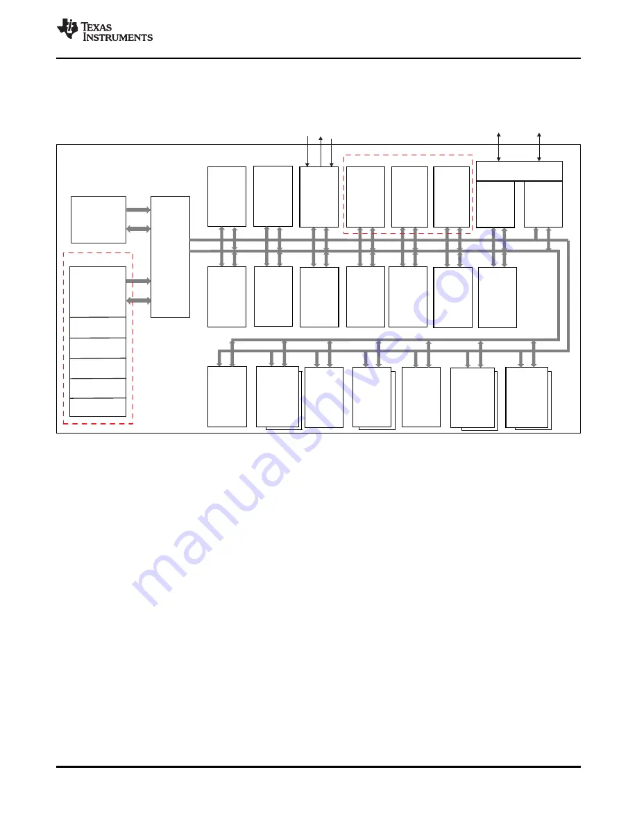
Functional Block Diagram
shows the functional block diagram of the MSP432P401R and MSP432P401M devices.
Figure 1-1. MSP432P401R, MSP432P401M Functional Block Diagram
The CPU and all of the peripherals in the device interact with each other through a common AHB matrix.
In some cases, there are bridges between the AHB ports and the peripherals. These bridges are
transparent to the application from a memory map perspective and, therefore, are not shown in the block
diagram.