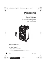
background image

HCD-MD555

US Model

AEP Model

UK Model

E Model

Tourist Model

Model Name Using Similar Mechanism

NEW

CD Section

CD Mechanism Type

CDM53-K1BD33

Optical Pick-up Type

KSM-213BFN/C2NP

Model Name Using Similar Mechanism

NEW

MD Section

MD Mechanism Type

MDM-C1E

Base Unit Type

MBU-C1E

Optical Pick-up Type

KSM-260A/J1N

• This set is the Amplifier, CD player,

MD Deck and Tuner section in
DHC-MD555.

SPECIFICATIONS

Manufactured under license from Dolby Laboratories
Licensing Corporation.
“DOLBY” the double-D symbol 

a

 “AC-3” and “PRO

LOGIC” are trademarks of Dolby Laboratories
Licensing Corporation.

MINI Hi-Fi COMPONENT SYSTEM

— Continued on next page —

Sony Corporation

Home Audio Company

Shinagawa Tec Service Manual Production Group

9-922-976-12

2001H1600-1

© 2001.8

SERVICE MANUAL

Ver 1.1  2001. 08

Summary of Contents for HCD-MD555

Page 1: ...ck up Type KSM 260A J1N This set is the Amplifier CD player MD Deck and Tuner section in DHC MD555 SPECIFICATIONS Manufactured under license from Dolby Laboratories Licensing Corporation DOLBY the double D symbol a AC 3 and PRO LOGIC are trademarks of Dolby Laboratories Licensing Corporation MINI Hi Fi COMPONENT SYSTEM Continued on next page Sony Corporation Home Audio Company Shinagawa Tec Servic...

Page 2: ...ick up block Therefore when checking the laser diode emission observe from more than 30 cm away from the objective lens Notes on chip component replacement Never reuse a disconnected chip component Notice that the minus side of a tantalum capacitor may be dam aged by heat Flexible Circuit Board Repairing Keep the temperature of the soldering iron around 270 C dur ing repairing Do not touch the sol...

Page 3: ...metal part having a return to chassis must not exceed 0 5 mA 500 microampers Leakage current can be measured by any one of three methods 1 A commercial leakage tester such as the Simpson 229 or RCA WT 540A Follow the manufacturers instructions to use these instruments 2 A battery operated AC milliammeter The Data Precision 245 digital multimeter is suitable for this job 3 Measuring the voltage dro...

Page 4: ... 3 Schematic Diagram CD Section 63 7 4 Printed Wiring Board CD Section 65 7 5 Schematic Diagram Motor Section 67 7 6 Printed Wiring Board Motor Section 69 7 7 Printed Wiring Board MD Section 71 7 8 Schematic Diagram MD Section 1 2 73 7 9 Schematic Diagram MD Section 2 2 75 7 10 Schematic Diagram Rds Section 77 7 11 Printed Wiring Board Rds Section 78 7 12 Schematic Diagram Relay Section 79 7 13 Pr...

Page 5: ... or p to let Check appear 2 Turn the MULTI JOG to display Service and press the ENTER YES button 3 Turn the MULTI JOG to display ERR DP MODE 4 Press the ENTER YES button to enter the error history mode and the message total rec appears 5 Select the item to be displayed or to be executed using the MULTI JOG 6 When you want to display or execute the selected item press the MULTI JOG 7 If you press t...

Page 6: ...rror No er refresh 3 This is the mode with which you can clear the histories of retry err total err and err history Perform this operation to clear the past error history before returning the repaired product to the customer To clear the error histories press the MULTI JOG button After er refresh is displayed press the ENTER YES button The error histories are cleared and the message Complete appea...

Page 7: ...l error count CD2 6 Resets the NO DISC count Note 1 Mechanical error code a Mechanical error count The latest error 00 to the last ten error 09 b FF Mechanical error after mechanism is initialized c 1 Mechanical error during loading the tray in between 2 the stocker position and the deeper end d Don t care e 2 Mechanism error while the stocker is moving up down f 2 Mechanism error of the clumper a...

Page 8: ...haracters will not be displayed properly These will be displayed as a space or a character resembling it Table 1 CD TEXT TEST DISC Recorded Data Contents and Display TRACKS No 1 to 32 Normal Characters Other channel is infinity zero TRACK No Recorded contents Display 1 2 3 4 5 6 7 8 9 10 11 12 13 14 15 16 17 18 19 20 21 22 23 24 25 26 27 28 29 30 31 32 1kHz 0dB L R 20Hz 0dB L R 40Hz 0dB L R 100Hz ...

Page 9: ...n TRACK Recorded contents Display 33 34 35 36 37 38 39 40 41 42 43 44 45 46 47 48 49 50 51 52 53 54 55 56 57 58 59 60 61 62 63 64 65 66 67 to 99 100Hz 0dB R 1kHz 0dB R 10kHz 0dB R 20kHz 0dB R 100H square wave L R 1Hz square wave L R 1kHz emphasis ON 0 37dB L R 5kHz emphasis ON 4 53dB L R 16kHz emphasis ON 9 04dB L R 21h to 27h 1kHz 0dB L R 28h to 2Fh 0 1 2 3 4 5 6 7 30h to 37h 8 9 38h to 3Fh A B C...

Page 10: ...dicated on the optical pickup as follows Selection of numeral Select a number by turning the MULTI JOG dial Selection of digit Select the desired digit by pressing the MD WALKMAN SYNC button 6 Press the ENTER YES button and the message Measu appears is an arbitrary number 7 Press the ENTER YES button without changing the number because the result data of adjustment is saved as the value of step 6 ...

Page 11: ...re arbitrary numbers Cleaning the optical pickup Re adjustment Replacement of the optical pickup Replacement of the optical pickup Replacement of the optical pickup Replacement of the optical pickup Replacement of the optical pickup When test result is all the time defective Replacement of the over write head Check that circuits in the peripheral of the over write head are not open When test resul...

Page 12: ...D WALKMAN SYNC button GROOVE button PLAY MODE TUNNING MODE button 1 ALL button REPEAT STEREO MONO button VOLUME dial CLEAR button ENTER YES button CD1 6 CD5 6 buttons ª MENU NO button º MULTI JOG dial PRESET EQ button NAME EDIT CHARACTER button FUNCTION button REC IT button HIT PARADE button SEAMLESS button SELECT SYNC button CD1 CD5 p buttons ª TIMER SELECT button º SET button 1 u power button 1 ...

Page 13: ... 13 This section is extracted from instruction manual ...

Page 14: ... 14 ...

Page 15: ... 15 ...

Page 16: ... 16 ...

Page 17: ... 17 ...

Page 18: ... 18 ...

Page 19: ... 19 ...

Page 20: ... 20 ...

Page 21: ... 21 ...

Page 22: ... 22 ...

Page 23: ... 23 ...

Page 24: ... 24 ...

Page 25: ... order given 4 1 BACK PANEL Remove the upper cover first 4 2 MECHANISM MDM C1E 5 Three connectors 6 Back panel 2 Cover Back 3 Ten screws BV 3 8 4 Seven screws BV 3 8 1 Three screws BV 3 8 4 Cover MDM 6 MD mechanism MDM C1E 1 TUNER 5 Three screws BV 3 8 3 Screw BV 3 8 2 Screw BV 3 8 ...

Page 26: ...or 4 Two connectors 1 Two connectors 8 AMP board 3 SP board º Heat sink Back panel REG board TRANS D board JE HK SP MY MODEL 4 Two screws BV 3 8 Three screws BV 3 8 º Front panel 7 Connector 1 Two connectors 5 Holder WLS 10 Remove the holder from the MAIN board 6 Connector 9 MAIN board 2 Flat type wire 19 core 3 Flat type wire 17 core 8 Flat type wire 29 core Abbreviation HK Hong Kong SP Singapore...

Page 27: ... BVTP 2 6 8 º Four screws BVTP 2 6 8 Three screws BVTP 2 6 8 3 Two screws BVTP 2 6 8 7 Screw BVTP 2 6 8 PANEL board Front panel 8 LED board 6 POWER KEY board 2 Chassis MD 4 Bracket MD chassis 2 Three screws BV 3 10 1 Four screws BVTT 3 8 6 TRANS B board 7 TRANS C board 5 TRANS A board 4 Two connectors 8 Chassis Transformer 3 Power transformer T960 ...

Page 28: ... 28 4 7 CD MECHANISM CDM53 K1BD33 2 Two screws BV 3 8 1 Two screws BV 3 8 3 CD mechanism CDM53 K1BD33 Chassis ...

Page 29: ...8 Lever S assy 6 Cover FFC 9 Bracket To assemble the bracket refer to the following note 4 Flat type wire 13 core 3 Flat type wire 7 core 7 Screw BVTT 2 6 5 Screw BVTT 2 6 5 Lever S assy Bracket Note When assembling the bracket raise the lever S assembly engage it with the bracket and slide them in the direction of the arrow ...

Page 30: ...AD RELAY BOARD 8 HEAD RELAY board 2 Belt A 1 Connector 7 Remove soldering of the motor 6 Motor Head assy M905 Remove the motor assy in the direction of the arrow B 4 Chassis Head gear assy Remove the chassis assy in the direction of the arrow A B A 3 Screw BVTT 2 6 5 5 Two screws P 2 2 ...

Page 31: ...Connector 3 MD base unit MBU C1E Note Remove the MD base unit while being careful of the over write head Over write head 4 Two screws P 1 7 2 2 2 Connector 1 Flexible pc board 6 OP translation flexible pc board 7 BD board 3 Screw BVP 2 6 5 4 12 BD BOARD ...

Page 32: ...1 1 Screw P1 7 2 5 1 Screw M 1 7 1 4 2 Stopper 4 Optical pick up block KMS 260A JIN Remove the optical pickup block in the direction of the arrow 3 Shaft MAIN 4 13 OVER LIGHT HEAD HR901 4 14 MD OPTICAL PICK UP BLOCK KMS 260A J1N ...

Page 33: ...BA F NP 8 Four screws BVTP 2 6 7 Connector 9 Fitting base Magnet assy 5 Two screws BVTP 2 6 4 Two screws BVTP 2 6 6 Loading panel Chassis 2 Four screws BVTP 2 6 3 Fitting base Guide assy 1 Two connectors 4 15 CD OPTICAL PICK UP BLOCK KSS 213BA F NP 4 16 FITTING BASE GUIDE MAGNET ASSY ...

Page 34: ...UB 1 Turn the pulley LD and move the slider selection in the direction of the arrow L 2 Turn the pulley mode in the direction of the arrow to adjust the tray sub that you want to remove It depends on the height and position of the stocker 3 Turn the pulley LD and move the slider selection in the direction of the arrow R 4 Turn the pulley mode in the direction of the arrow so that you can remove th...

Page 35: ...ar so that the gear is positioned in line with the gear Gear B as shown in the figure Gear Gear B In line with this straight line 6 Two screws PTP WHM 2 6 5 Washer 4 Compression spring 7 Insert the slider selection to A portion 3 Protrusion of slider selection 1 Rotary encoder 2 Gear chucking A This portion must come into the groove of the rotary encoder Rotary encoder Two marks must be aligned Al...

Page 36: ...r selection A portion of the tray sub Tray Sub A 3 Three screws BVTP 2 6 1 Chassis Mold B Insert the A portion to the B portion of the slider selection A 2 Gear EJECT Insert the gear EJECT beneath the gear LD deceleration Gear LD deceleration B portion of the slider selection 4 21 HOW TO ATTACH THE STOCKER 4 22 HOW TO ATTACH THE CHASSIS MOLD B ...

Page 37: ...test mode is activated You can select the four test groups sequentially in order by rotating MULTI JOG N n Check N n Adjust N n Service N n Develop N n Method 2 Turn on the power and select the MD function Press the three buttons simultaneously i e the ENTER YES NAME EDIT and MD5 buttons to activate the test mode TEMP CHECK appears indicating that the test mode is activated When the test mode is a...

Page 38: ...s display D ERR DP MODE 17 Error history display clear S SLED MOVE 18 Sled check D ACCESS MODE 19 Access check D 0920 CHECK 20 Outermost circumference check D HEAD ADJUST 21 Head position check D CPLAY2 MODE 22 Same function as CPLAY MODE D CREC2 MODE 23 Same function as CREC MODE D ADJ CLEAR 24 Initialization of adjustment value in non volatile memory A S AG Set MO 25 Auto gain output level adjus...

Page 39: ...icates the error rate and ADER 2 How to Change the Playback Segment 1 If you press the ENTER YES button during continuous playback the display changes as shown below and a different segment can be played back CPLAY MID n CPLAY OUT n CPLAY IN 2 When access to the segment is completed the display changes to C AD Note The number in the area on the display indicates the error rate and ADER 3 Ending th...

Page 40: ...rned off 2 To remove the disc press the MD button Note 1 The recording start addresses for IN MID and OUT are as follows IN 40h cluster MID 300h cluster OUT 700h cluster Note 2 The MENU NO button remains valid at all times and can be used to stop recording at any time Note 3 Do not perform continuous recording for longer than 5 minutes Note 4 Be careful not to give vibration during continuous reco...

Page 41: ...gain display is as follows AG Detrack check display This display is not used during servicing The detrack check display is as follows ADR IVR display This display is not used during servicing The IVR display is as follows MEANING OF OTHER DISPLAYS Display Contents When turned on When turned off LED green During continuous playback CLV ON STOP CLV OFF P LED amber Tracking servo OFF Tracking servo O...

Page 42: ...not move down etc NG REC 5s Does not start recording NG BLANK ALL ERASE is attempted but resulted in fail Errors can be cleared by pressing the FR button and the aging restarts 4 Ending of aging Aging ends by pressing the MENU NO button TEST MODE DISPLAY 1 How to Enter the Test Mode While pressing the ENTER YES and REC buttons press the POWER button twice i e turn off the main power and back on ag...

Page 43: ...d ground are not shorted inside an oscilloscope VC and ground will be short circuited 5 When the above described BD board waveform check jig Part No J 2501 149 A is used to observe waveforms waveforms can be observed without soldering pickup flexible board laser tap 1 Initial setting of adjustment value 2 Saving the IOP information the value that is indicated on the pickup 3 Temperature compensati...

Page 44: ... on top of the objective lens of the optical pickup When it cannot be set properly press the 0 button or button to move the optical pickup so that the laser power meter can be set Connect the digital voltmeter to TP170 I 3 V and TP169 IOP 2 Rotate the MULTI JOG knob and let the display LDPWR CHECK C 2 appear 3 Press the ENTER YES button once and let the display LD 0 9 mW appear Check that the lase...

Page 45: ... Specified value Offset value 10 or less Offset value 100 A B 2 A B VC A B Traverse waveform Specified value Offset value 10 or less Offset value 100 10 Observe waveform on an oscilloscope to confirm that waveform on an oscilloscope satisfies the specified value Do not rotate the MULTI JOG knob at this time 11 Press the ENTER YES button and let the display EF MO CHECK appear The disc stops rotatin...

Page 46: ... the check disc MD Self Record Playback Check The set that is being repaired creates a continuous record playback disc by itself and checks the error rate Checking Method 1 Insert a disc blank disc to which data is allowed to be recorded 2 Rotate the MULTI JOG knob and let the display CREC MID S 31 appear 3 Press the ENTER YES button and let the display CREC MID appear 4 As recording is started th...

Page 47: ...ffset Adjustment Save the temperature data at that time in the non volatile memory as 25 C reference data Note 1 Usually do not perform this adjustment 2 Perform this adjustment in an ambient temperature of 22 C to 28 C Perform it immediately after the power is turned on when the internal temperature of the unit is the same as the ambient temperature 3 When D101 has been replaced perform this adju...

Page 48: ... This is just a display and any operations are not necessary Traverse Adjustment Connection Adjusting method 1 Connect an oscilloscope to TP233 TEO and TP416 VC of the BD board 2 Insert an MO disc any MO disc available on the market Refer to Note 1 3 Press the button and move the optical pickup toward outer circumference of the pit area 4 Rotate MULTI JOG and let the display EF MO ADJUST 11 appear...

Page 49: ...m Specification A B VC A B Traverse Waveform Specification A B TP233 TEO 10pF TP416 VC 330k Ω BD board Oscilloscope Focus Bias Adjustment Adjusting Method 1 Load a test disc MDW 74 AU 1 2 Rotate the MULTI JOG knob and display CPLAY MODE 29 3 Press the ENTER YES button twice and display CPLAY MID 4 Press the MENU NO button when C AD is displayed 5 Rotate the MULTI JOG knob and display FBIASADJUST 1...

Page 50: ...isplay a Check that the C1 error is below 220 and ADER is 2 9 Press the MENU NO button next press the MD button and remove the continuously recorded disc Note 1 If the C1 error and ADER are above 00 at points a step 8 or b step 7 the focus bias adjustment may not have been carried out properly Adjust perform the beginning again Auto Gain Control Output Level Adjustment Be sure to perform this adju...

Page 51: ...tor with neutral detergent when the signal level is low than specified value with the following checks S Curve Check Procedure 1 Connect oscilloscope to test point TP FEO on SERVO board 2 Connect between test point TP FEI and TP VC by lead wire 3 Connect TP AGCON to ground by lead wire 4 Turn U power switch on 5 Put disc YEDS 18 in and turn U power switch on again and actuate the focus search actu...

Page 52: ...n BD CD Board Side A BD MD Board Side A MAIN Board BD MD Board Side B TP VC TP AGCCON TP VC TP FEI TP TEO TP FEO TP RF IC102 IC101 IC103 IC302 IC300 IC100 CN300 TP308 IC316 TP169 TP170 TP233 IC121 IC124 IC101 D101 CN101 ...

Page 53: ... CLOCK GEN 27 28 29 XBCK LRCK FS256 DIGITAL SIGNAL SW MONITOR CONTROL INTERNAL BUS DRAM DRAM 43 47 46 44 XOE XWE XRAS XCAS 25 ADDT IC124 1 2 3 4 5 6 7 8 9 15 14 12 11 93 94 SPFD SPRD SQSY DQSY XINT TX SENS SRDT XLAT SCLK SWDT MNT0 MNT1 MNT2 MNT3 26 DADT MD MECHANISM CONT IC316 MNT0 82 MNT1 81 MNT2 80 MNT3 79 SWDT 35 SCLK 37 XLAT 66 SRDT 36 SENS 78 SCTX 72 XINT 73 DQSY 75 SQSY 27 LD ON 57 MOD 65 WR...

Page 54: ...TFDR TRDR FFDR FRDR SRDR SFDR XLON 14 VC 38 72 L OUT 75 R OUT 5 DATA R CH DATA 29 6 XLAT XLT 31 7 CLOK CLK 30 1 SQSO SUBQ 68 2 SQCK SQCK 70 9 SCLK 8 SENS SENS 74 20 SCOR SCOR 46 XTAI 66 XTAO 67 SSTP 27 X101 16 9344MHz S101 LIMIT 3 XRST BDRST 10 XMODE 71 CD MECHANISM CONT IC300 SRAM IC302 5 RE 6 OE 20 MID OUT SW 21 MID IN SW 19 IN SW 18 OUT SW 32 LID OUT SW 26 INIT SW 60 CNT SW S701 S703 S704 S708 ...

Page 55: ...K SWITCH Q100 MUTE Q101 MUTE CONT MUTE CONT POWER AMP IC801 Q101 Q510 511 Q505 D151 OVER LOAD DETECT Q801 OVER LOAD DETECT SWITCH Q833 DC IN DETECT Q831 832 RELAY DRIVE Q830 834 835 RY800 J20 PHONES TB800 R CH SPEAKER R CH 31 TUNED 30 STEREO 29 ST MUTE 32 ST CE 35 ST CLK 33 ST DOUT 34 ST DIN RDS AEP UK MODEL IC630 631 X630 4 332MHz R CH SPEANA IC502 17 16 15 14 4 3 SYSTEM CONTROL IC500 1 2 18 RDS ...

Page 56: ... LED DRIVER IC704 DATA 15 CLK 16 STB 17 CLR 18 83 LED CLEAR UPPER LOWER SWITCH Q914 917 920 921 Q919 Q918 33V SWITCH Q960 961 VF COM VF LOWER VF UPPER VG 33V FL DRIVER Q918 Q963 POWER CONTROL Q504 5V REG IC960 1 3 D500 D501 RESET IC501 1 3 SUB 5V SYSCON D966 969 D960 963 T961 5V REG IC901 1 3 BACKUP SWITCH 5V REG IC902 1 3 B SWITCH Q911 912 913 Q501 503 Q505 507 MD 5V CD 5V HEAD 5V 5V REG Q908 909...

Page 57: ...l resistors are in Ω and 1 4 W or less unless otherwise specified indicates tolerance internal component 2 nonflammable resistor 1 fusible resistor C panel designation U B Line V B Line Voltages are taken with aVOM Input impedance 10 MΩ Voltage variations may be noted due to normal produc tion tolerances Waveforms are taken with a oscilloscope Voltage variations may be noted due to normal produc t...

Page 58: ... Refer to page 103 for Waveforms Refer to page 105 for IC Block Diagrams Refer to page 111 112 for IC Pin Function Description The components identified by mark or dotted line with mark are critical for safety Replace only with part number specified ...

Page 59: ...CD SECTION 65 66 Refer to page 61 for Circuit Boards Location VC RF TEO FEO AGC CON FEI VC Page 84 23 C129 C143 1 2 A B C D E F G H 3 4 5 6 7 8 9 10 11 12 16 Ref No Location IC101 E 3 IC102 C 2 IC103 D 2 Q101 F 12 Semiconductor Location ...

Page 60: ...HCD MD555 7 5 SCHEMATIC DIAGRAM MOTOR SECTION 67 68 Refer to page 109 for IC Block Diagrams RT1N141S TP MTZJ T 72 5 1B ...

Page 61: ...HCD MD555 7 6 PRINTED WIRING BOARD MOTOR SECTION 69 70 Refer to page 61 for Circuit Boards Location Page 83 Page 83 1 2 A B C D E F G H I J 3 4 5 6 7 8 9 10 11 12 13 14 16 ...

Page 62: ... 5 6 7 8 9 10 11 12 16 Page 81 Page 84 Page 84 Page 81 Page 82 Ref No Location D101 B 10 D181 F 12 D183 F 12 IC101 B 4 IC103 B 2 IC121 D 4 IC124 C 5 IC152 D 2 IC171 E 3 IC172 F 3 IC181 F 2 IC191 D 9 IC200 E 11 IC201 F 5 IC316 E 4 IC401 D 6 Q101 C 3 Q102 B 3 Q103 C 2 Q104 C 3 Q162 C 2 Q163 B 2 Q181 F 11 Q182 F 11 Q401 C 8 Q402 C 8 Q403 C 8 Semiconductor Location ...

Page 63: ...o page 104 for Waveforms Refer to page 106 107 for IC Block Diagrams Refer to page 113 to 116 for IC Pin Function Description RN2304 TE85 K The components identified by mark or dotted line with mark are critical for safety Replace only with part number specified ...

Page 64: ...9 SCHEMATIC DIAGRAM MD SECTION 2 2 75 76 Refer to page 71 for IC Block Diagrams Refer to page 106 for Waveforms Refer to page 108 for IC Block Diagrams Refer to page 107 to 119 for IC Pin Function Description 205C ...

Page 65: ... 10 SCHEMATIC DIAGRAM RDS SECTION 7 11 PRINTED WIRING BOARD RDS SECTION 77 78 Refer to page 110 for IC Block Diagrams Refer to page 120 for IC Pin Function Description Refer to page 61 for Circuit Boards Location ...

Page 66: ...HCD MD555 7 12 SCHEMATIC DIAGRAM RELAY SECTION 79 80 Refer to page 108 for IC Block Diagrams UN4213 TA 390 390 ...

Page 67: ...HCD MD555 7 13 PRINTED WIRING BOARD RELAY SECTION 81 82 Refer to page 61 for Circuit Boards Location 16 Page 72 Page 72 Page 71 1 2 A B C D E F G H I J 3 4 5 6 7 8 9 10 11 12 13 14 ...

Page 68: ... D903 H 6 D904 F 7 D906 H 6 D907 H 6 D908 H 5 D909 H 3 D910 G 3 D911 G 3 D914 I 4 D915 G 2 D916 G 4 D923 I 4 D924 C 7 D926 E 5 IC100 D 9 IC300 G 9 IC301 F 9 IC302 H 8 IC400 B 4 IC402 I 11 IC403 C 2 IC405 C 1 IC500 C 4 IC501 D 3 IC502 C 8 IC503 C 6 IC504 H 11 IC900 H 4 IC901 F 4 IC902 F 4 IC903 F 6 IC904 E 5 Q100 E 8 Q101 E 7 Q200 D 8 Q201 D 7 Q300 G 8 Q301 F 10 Q400 C 2 Q401 C 1 Q403 B 2 Q404 B 2 ...

Page 69: ...15 SCHEMATIC DIAGRAM MAIN SECTION 1 3 Refer to page 109 for IC Block Diagrams L R L R L R 133 3 9 The components identified by mark or dotted line with mark are critical for safety Replace only with part number specified ...

Page 70: ...D MD555 87 88 7 16 SCHEMATIC DIAGRAM MAIN SECTION 2 3 Refer to page 83 for Printed Wiring Board Refer to page 104 for Waveforms Refer to page 123 124 for IC Pin Function Description JR404 0 JR403 0 5 6 10 ...

Page 71: ... for Printed Wiring Board Refer to page 104 for Waveforms Refer to page 109 for IC Block Diagrams Refer to page 121 122 for IC Pin Function Description The components identified by mark or dotted line with mark are critical for safety Replace only with part number specified ...

Page 72: ...HEMATIC DIAGRAM AMP SECTION 133 133 133 133 UN4112 TA C21 0 001 C20 0 001 0 1 180 1 4W 133 L R SREAKER The components identified by mark or dotted line with mark are critical for safety Replace only with part number specified ...

Page 73: ... Page 101 Page 83 SPEAKER R L 1 2 A B C D E F G H 3 4 5 6 7 8 9 10 11 12 16 Ref No Location D801 C 5 D802 D 5 D830 C 6 D851 C 2 D852 C 2 D891 F 4 IC801 A 4 Q801 C 4 Q830 C 2 Q831 E 2 Q832 E 2 Q833 D 2 Q834 F 2 Q835 D 2 Q851 C 2 Q990 E 11 Q991 F 10 Q992 F 10 Q993 F 10 Q994 F 10 Semiconductor Location ...

Page 74: ...HCD MD555 95 96 7 20 SCHEMATIC DIAGRAM PANEL SECTION Refer to page 110 for IC Block Diagrams ...

Page 75: ...1 12 16 Ref No Location D701 H 12 D702 H 10 D703 H 6 D704 I 5 D705 I 5 D707 H 3 D708 F 3 D709 D 2 D710 B 4 D711 B 5 D712 H 5 D713 G 5 D714 F 5 D715 F 5 D716 E 5 D717 D 5 D718 H 4 D719 G 4 D720 F 4 D721 F 4 D722 E 4 D723 D 4 D724 B 10 D725 B 10 IC701 G 7 IC702 D 7 IC703 G 2 IC704 D 2 IC705 I 7 Q701 G 7 Q702 G 6 Q703 C 8 Q704 C 8 Q705 I 7 Q706 H 11 Q707 H 11 Q708 H 11 Semiconductor Location ...

Page 76: ...9 100 7 22 SCHEMATIC DIAGRAM POWER SECTION The components identified by mark or dotted line with mark are critical for safety Replace only with part number specified 2 5A 250V 4A 125V F960 EXCEPT US MODEL US MODEL ...

Page 77: ... No Location D960 C 7 D961 C 7 D962 C 7 D963 C 8 D964 D 7 D965 D 7 D966 D 8 D967 E 8 D968 D 8 D969 D 8 D970 E 7 D971 C 6 D972 E 8 D973 E 8 D974 E 6 D976 H 8 IC960 F 7 Q960 C 6 Q961 C 7 Q963 C 6 Q964 F 8 Semiconductor Location F960 US MODEL EXCEPT US MODEL 1 2 A B C D E F G H I J 3 4 5 6 7 8 9 10 11 12 13 16 ...

Page 78: ...16 9344 MHz 138 µs 5 Vp p BD MD Section 400 mVp p 1 IC101 RF MD PLAY 2 5 µs 4 Vp p 4 1 Vp p 2 5 µs 4 Vp p 90 ns 2 IC152 CAPA MD PLAY 3 IC152 CAPA MD PLAY 4 IC121 ª FS256 5 IC121 XBCK 6 IC121 LRCK 7 IC121 OSCI 8 IC316 XIN MAIN Section 1 IC300 X2 4 Vp p 350 ns 23 µs 4 Vp p 1 9 Vp p 22 5792 MHz 2 4 Vp p 10 MHz 4 4 Vp p 12 5 MHz 4 4 Vp p 32 768 kHz 3 4 Vp p 12 5 MHz 2 IC500 XT2 3 IC500 X2 ...

Page 79: ...T AVSS1 AVSS2 CPU INTERFACE SERVO AUTO SEQUENCER SERIAL IN INTERFACE OVER SAMPLING DIGITAL FILTER 3rd ORDER NOISE SHAPER PWM PWM EFM DEMODULATOR TIMING LOGIC DIGITAL OUT D A INTERFACE DIGITAL PLL ASYMMETRY CORRECTION CLOCK GENERATOR MIRR DFCT FOK DETECTOR DIGITAL CLV SUBCODE PROCESSOR SERVO INTERFACE SERVO DSP FOCUS SERVO TRACKING SERVO SLED SERVO PWM GENERATOR FOCUS PWM GENERATOR TRACKING PWM GEN...

Page 80: ...25 WBLADJ 24 VCC 23 3TADJ 22 EQADJ 21 VREF 20 F0CNT 19 XSTBY 18 XLAT 17 SCLK 16 SWDT 15 TEMPR 14 TEMPI 13 GND 12 APCREF 11 APC 10 PD 9 F 8 E 7 D 6 C 5 B 4 A 3 VC VI CONV BGR VREF SCRI PARA DECODE AUXSW COMMAND IVR GSW FF FBAL FF TG SEA 1 2 TG TEA WBL 3T EQ DET ADIP AGC WBL BPF22 BPFC ABCDA FEA WBL ATA CVB RFA1 1 2 1 2 GRVA OFST RFA2 GRV HLPT PTGR 2 1 1 2 BOTTOM PEAK RF AGC EQ EQ DET P P WBL 3T WBL...

Page 81: ...SCO 16 OSCI 15 TX 14 XINT 13 RECP 12 DQSY 11 SQSY 10 XRST 9 SENS 8 SRDT 7 XLAT 6 SCLK 5 SWDT 4 MNT3 3 MNT2 2 MNT1 1 MNT0 PWM GENERATOR AUTO SEQUENCER SERVO DSP CPU I F MONITOR CONTROL SPINDLE SERVO EACH BLOCK EACH BLOCK DIGITAL AUDIO I F SAMPLING RATE CONVERTER CLOCK GENERATOR SUBCODE PROCESSOR EACH BLOCK A D CONVERTER ANALOG MUX EFM ACIRC ENCODER DECODER PLL SHOCK RESISTANT MEMORY CONTROLLER ATRA...

Page 82: ... 3 VINR1 4 VADCN 5 VINL2 6 VADCP 7 VINR2 8 OVERFL 9 VDDD 10 VSSD 11 SYSCLK 12 L3MODE 13 L3CLOCK VREF VSS DAC VOUTL VDD DAC VOUTR QMUTE AGCSTAT TEST2 TEST1 DATAI DATAO WS BCK L3DATA 14 28 27 26 25 24 23 22 21 20 19 18 17 16 15 0dB 6dB SWITCH ADC1L 0dB 6dB SWITCH ADC1R PGA ADC2L PGA ADC2R DAC DAC DIGITAL AGC DIGITAL INTERFACE DIGTAL MIXER DECIMATION FILTER DSP FEATURES INTERPOLATION FILTER NOISE SHA...

Page 83: ...C 8 NC 9 NC 4 16 f02 17 f01 18 RESET RESET C PREF LINE NF LINE IN REFFERENCE CURRENT BPF DET BPF DET BPF DET BPF DET DET RESET Bias IC504 P82B715TD 1 2 3 4 GND SX LX NC BUFFER 8 7 6 5 NC SY LY VCC BUFFER CLAMP MOTOR Section LAD MOTOR Section IC701 M54641L CLAMP MOTOR Section IC702 M54641L LAD MOTOR Section 1 5 2 7 3 6 4 POWER AMP POWER AMP CONTROL INPUT AMP INPUT AMP REG 8 VCC VCC REFERENCE OUT2 O...

Page 84: ...C D0 D1 CNVSS VSS D6 D7 D4 D5 D3 D2 36 35 34 33 32 31 30 29 28 27 26 25 24 23 22 21 20 19 18 17 16 15 14 13 12 11 10 9 8 7 6 5 4 3 2 1 CLOCK GEN CONTROL SIGNAL CARRY CARRY ALU REGISTER C 2 REGISTER HA 4 REGISTER LA 4 ADF 1 A D CONV MPX INTE 1 EXF 1 4 9 4 2 PORT S 4 4 4 4 4 4 4 4 3 4 7 10 6 10 9 9 7 3 2 8 8 4 8 4 PORT D 9 MULTIPLEXER PORT F 4 REGISTER H 4 REGISTER L 4 REGISTER J 4 SERIAL I O SIOF 1...

Page 85: ...utput MNT2 XROF output when selected command C2PO output MNT3 GTOP output when selected command H output when either subcode sync S0 or S1 is detected Not used Number of tracks counting signal input output Mirror signal input output Defect signal input output Focus OK signal input output GFS is sampled by 460 Hz H output when GFS is H L output when GFS is L eight times continuously Input mode when...

Page 86: ...erminal Power supply Digital Out output terminal D A interface LR clock output f Fs D A interface Serial data output 2 s complement MSB first D A interface Bit clock output H output when playback disc has emphasis L output when playback disc has no emphasis Not used Oscillation circuit power supply Crystal oscillation circuit input terminal When master clock is input from external source it is inp...

Page 87: ... error signal output to CXD2654AR IC121 External low pass filter capacitor of the sled error signal is connected to this terminal Sled error signal output to CXD2654AR IC121 FM signal output of ADIP ADIP FM signal input with AC coupling External AGC capacitor for ADIP is connected to this terminal ADIP duplex FM signal 22 05 kHz 1 kHz output to CXD2654AR IC121 Auxiliary signal I3 signal temperatur...

Page 88: ... head on off output System clock 512Fs 22 5792 MHz input System clock 512Fs 22 5792 MHz input open in this set Input signal for setting the system clock frequency L 45 158 MHz H 22 5792 MHz Fixed at H in this set Digital audio input signal for recording Either digital signal or optical input from CD is selected in this set DIN1 is not used in this set Digital audio signal output during playback mo...

Page 89: ...nput from the CXA2523AR IC101 Focus error signal input from the CXA2523AR IC101 Auxiliary signal I3 signal temperature signal input from the CXA2523AR IC101 Center point voltage 1 65 V input from the CXA2523AR IC101 Monitor output of the A D converter input signal Not used in this set Power supply terminal 3 3 V analog system A D converter operation range s upper limit voltage input fixed at H in ...

Page 90: ...t terminal X tal system Not used in this set open Sled servo drive PWM signal output to the BH6511FS IC152 Sled servo drive PWM signal output to the BH6511FS IC152 Spindle servo drive PWM signal output to the BH6511FS IC152 Spindle servo drive PWM signal output to the BH6511FS IC152 FG signal output Not used in this set fixed at L TEST input terminals fixed at L Ground terminal digital system The ...

Page 91: ...erminal 3 3 V NMI input Not used in this unit fixed at H Power down detection input terminal L is input when voltage decreases Sync input from the MD WALKMAN I2C bus busy signal output L3 bus clock output L3 bus data output Elevator up signal output Elevator down signal output Subcode Q sync SCOR input from CXD2654AR IC121 L is output every 13 3 mseconds H is output in most cases Reset input I2C b...

Page 92: ... Playback position detection switch input Not used in this set open Control signal output of the recording playback status Not used in this set open Power supply terminal 3 3 V Sled limit in detection switch S681 input L sled limit in when the optical pickup comes to the innermost circumference Ground terminal Laser modulation selector signal output to the HF modulation switch circuit During playb...

Page 93: ...o the non volatile memory IC171 Bi directional data bus to the non volatile memory IC171 Disc detection signal input Input from the over write head DOWN position detector switch S7 L is input when the over write head is at the DOWN position Input from the over write head UP position detector switch S6 L is input when the over write head is at the UP position Key input terminal Ground terminal Key ...

Page 94: ...loaded into the stocker Input signal from the detection switch S703 MID IN of the CD mechanism deck L During the moment when the sub tray moves away from the tray until it is loaded to the stocker TEST input terminal fixed at L in this set Input signal from the roatery encoder S707 of the CD mechanism deck Input signal from the detection switch S705 INIT of the CD mechanism deck L When the tray ar...

Page 95: ...c H Composite mode L separate model fixed at H in this set FOCUS NO DISC is selected at GFS NG during search Input signal from the disc sensor Q703 of the CD mechanism H disc is present Input signal from the detection switch S706 COUNT of the CD mechanism deck L When elevator arrives at each sub try storing position Ground terminal for A D converter Not used fixed at L Not used in this set open Re...

Page 96: ... tuner Enable signal output to tuner Data output to tuner Data input for tuner Clock output to tuner Not used in this set Power supply terminal External crystal is connected to this terminal Ground terminal External crystal is connected to this terminal Reset input Clock output Data output AC cutting signal output Remote control Y bus clock input Y bus clock output Y bus busy signal output Pin Nam...

Page 97: ...OB JOG 6 4 925 161 81 EMBLEM 4 A SONY 7 4 212 226 02 LID MD 8 4 212 227 02 BASE LID 9 4 989 453 11 CUSHION LID 10 4 212 247 01 PLATE LIGHT GUIDE 11 3 354 963 21 DAMPER 12 4 951 620 01 SCREW 2 6 8 BVTP 13 X 4950 345 1 PANEL ASSY FRONT JE US HK SP MY 13 X 4950 420 1 PANEL ASSY FRONT AEP UK 14 X 4950 325 1 BRACKET CD LID L ASSY 15 X 4950 326 1 BRACKET CD LID R ASSY 16 X 4950 327 1 BRACKET MD LID ASSY...

Page 98: ...AEP UK HK SP MY 60 1 783 532 41 CORD POWER US 61 3 703 244 00 BUSHING 2104 CORD US AEP UK HK SP MY 61 3 703 571 11 BUSHING S 4516 CORD JE 62 4 212 204 11 PANEL BACK AEP UK 62 4 212 204 21 PANEL BACK SP MY 62 4 212 204 31 PANEL BACK HK 62 4 212 204 41 PANEL BACK US 62 4 212 204 51 PANEL BACK JE 63 1 500 021 11 CLAMP SLEEVE FERRITE 64 4 812 134 00 RIVET DIA 3 5 NYLON 65 1 569 007 11 ADAPTOR CONVERSI...

Page 99: ... 01 LOCK 98 NEW 109 1 671 472 01 DISK SW BOARD 111 4 988 375 01 RACK L 112 1 671 468 01 MECH RELAY BOARD 113 1 671 470 01 HEAD RELAY BOARD 114 3 661 080 00 BELT A 115 3 701 438 21 WASHER E 2 3 NYLON 116 3 018 636 01 GEAR PULLEY C 117 3 018 203 01 GEAR HEAD A 118 3 018 204 01 GEAR HEAD B 119 X 3374 348 1 CHASSIS HEAD GEAR ASSY 120 4 987 242 01 GEAR CAM 121 4 987 241 01 LEVER H 122 4 996 395 02 SPRI...

Page 100: ...62 4 986 952 01 GEAR 5 163 X 4949 171 1 CHASSIS ELEVATOR NEW ASSY 164 1 667 955 11 PC BOARD FLEXIBLE 165 4 986 948 01 GEAR 1 166 X 4949 225 3 BRACKET 1BN ASSY 167 4 986 953 01 WORM 168 1 671 469 01 ELEVATOR RELAY BOARD 169 1 782 909 11 WIRE FLAT TYPE 13 CORE 170 X 4947 928 1 BRACKET 1A ASSY 171 4 986 950 01 GEAR 3 172 4 987 244 01 SHAFT 1 173 4 986 949 11 GEAR 2 174 4 987 235 01 CLAMP B 175 3 326 ...

Page 101: ... 987 061 01 SPACER RACK 209 4 955 841 11 SCREW 210 4 979 906 11 SPRING LEAD SCREW 211 3 342 375 11 SCREW M1 7 1 4 SPECIAL 212 4 988 702 01 SHAFT MAIN 213 4 988 484 01 STOPPER 214 A 3304 200 A SCREW ASSY LEAD 215 4 983 511 02 PIN OUTSERT 217 4 908 618 21 SCREW BTP 2 6 218 4 967 688 11 MAGNET ABSORPTION 219 4 979 914 01 SPRING CLV TORSION 220 4 996 088 01 SPRING AU3 HR901 1 500 489 14 HEAD OVER LIGH...

Page 102: ...TING 257 A 4672 622 E BASE GUIDE ASSY FITTING 258 1 671 503 12 OUT SW BOARD 259 1 671 789 12 SENSOR 2 BOARD 261 A 4672 600 B MAGNET ASSY CHUCKING 262 1 671 505 12 IN SW BOARD 263 A 4672 623 C BASE MAGNET ASSY FITTING 264 4 211 235 01 BELT COMMUNICATION 265 4 211 236 01 BELT LOADING 266 4 211 228 01 LEVER GOOSENECK 267 4 211 231 01 PULLEY MODE 268 4 211 214 01 PULLEY LD 269 4 211 227 01 GEAR LD DEC...

Page 103: ...316 4 211 215 01 GEAR EJECT 317 4 211 245 01 SPRING COMPRESSION 318 4 211 221 01 GEAR LD MOVABLE 319 4 211 217 02 GEAR SELECTION 320 4 211 242 01 SHAFT SELECTION GEAR 321 1 418 045 01 ENCODER ROTARY 322 4 211 240 01 GEAR LD DECELERATION B 323 4 211 216 01 GEAR RELAY 324 4 211 241 01 LEVER SELECTION 326 4 211 218 01 GEAR GEAR A 327 4 211 219 01 GEAR GEAR B 328 4 211 220 01 GEAR U D SLIDER 329 1 671...

Page 104: ...01 8 848 379 31 OPTICAL PICK UP BLOCK KSM 213BFN C2NP 405 A 4724 330 A BD CD BOARD COMPLETE 406 1 769 069 11 WIRE FLAT TYPE 16 CORE 8 8 OPTICAL BLOCK BU K1BD33 407 4 996 243 11 SCREW M2 PSW 408 4 216 878 01 COLLAR The components identified by mark or dotted line with mark are critical for safety Replace only with part number specified ...

Page 105: ...42V C893 1 136 165 00 FILM 0 1uF 5 50V C894 1 136 165 00 FILM 0 1uF 5 50V CONNECTOR CN801 1 564 518 11 PLUG CONNECTOR 3P CN802 1 564 519 11 PLUG CONNECTOR 4P CN803 1 564 520 11 PLUG CONNECTOR 5P CN804 1 564 524 11 PLUG CONNECTOR 9P CN805 1 691 767 11 PLUG MICRO CONNECTOR 5P CN807 1 564 518 11 PLUG CONNECTOR 3P DIODE D801 8 719 911 19 DIODE 1SS119 D802 8 719 911 19 DIODE 1SS119 D830 8 719 911 19 DI...

Page 106: ...CERAMIC CHIP 0 1uF 25V C151 1 163 235 11 CERAMIC CHIP 22PF 5 50V C153 1 163 038 91 CERAMIC CHIP 0 1uF 25V C154 1 110 501 11 CERAMIC CHIP 0 33uF 10 16V C156 1 163 235 11 CERAMIC CHIP 22PF 5 50V C157 1 163 009 11 CERAMIC CHIP 0 001uF 10 50V C159 1 163 019 00 CERAMIC CHIP 0 0068uF 10 50V C161 1 126 206 11 ELECT CHIP 100uF 20 6 3V C162 1 126 205 11 ELECT CHIP 47uF 20 6 3V C163 1 126 206 11 ELECT CHIP ...

Page 107: ...06 11 ELECT CHIP 100uF 20 6 3V C140 1 163 227 11 CERAMIC CHIP 10PF 0 5PF 50V C142 1 163 251 11 CERAMIC CHIP 100PF 5 50V C143 1 163 251 11 CERAMIC CHIP 100PF 5 50V C144 1 163 251 11 CERAMIC CHIP 100PF 5 50V C148 1 163 227 11 CERAMIC CHIP 10PF 0 5PF 50V C151 1 126 206 11 ELECT CHIP 100uF 20 6 3V C152 1 163 038 91 CERAMIC CHIP 0 1uF 25V C153 1 163 021 91 CERAMIC CHIP 0 01uF 10 50V C156 1 163 038 91 C...

Page 108: ...SK1764KY Q401 8 729 402 42 TRANSISTOR UN5213 Q402 8 729 402 42 TRANSISTOR UN5213 Q403 8 729 402 42 TRANSISTOR UN5213 RESISTOR R103 1 216 049 91 RES CHIP 1K 5 1 10W R104 1 216 073 00 METAL CHIP 10K 5 1 10W R105 1 216 065 91 RES CHIP 4 7K 5 1 10W R106 1 216 133 00 METAL CHIP 3 3M 5 1 10W R107 1 216 113 00 METAL CHIP 470K 5 1 10W R110 1 216 073 00 METAL CHIP 10K 5 1 10W R112 1 216 089 91 RES CHIP 47K...

Page 109: ...5 1 10W R810 1 216 025 91 RES CHIP 100 5 1 10W R811 1 216 025 91 RES CHIP 100 5 1 10W R812 1 216 025 91 RES CHIP 100 5 1 10W R813 1 216 025 91 RES CHIP 100 5 1 10W R814 1 216 085 00 METAL CHIP 33K 5 1 10W R816 1 216 067 00 METAL CHIP 5 6K 5 1 10W R817 1 216 067 00 METAL CHIP 5 6K 5 1 10W R821 1 216 025 91 RES CHIP 100 5 1 10W R822 1 216 025 91 RES CHIP 100 5 1 10W R823 1 216 025 91 RES CHIP 100 5 ...

Page 110: ...50V C571 1 115 871 11 ELECT 1uF 20 50V C572 1 163 063 00 CERAMIC CHIP 0 022uF 50V CONNECTOR CN570 1 568 832 11 SOCKET CONNECTOR 13P CN571 1 568 848 11 SOCKET CONNECTOR 5P CN572 1 568 848 11 SOCKET CONNECTOR 5P IC IC570 8 759 982 73 IC BA10393F PHOTO INTERUPTER PH570 8 749 012 33 PHOTO INTERRUPTER GP1S94 PH571 8 749 012 33 PHOTO INTERRUPTER GP1S94 TRANSISTOR Q570 8 729 030 02 TRANSISTOR DTC144ESA R...

Page 111: ...0V C22 1 163 038 91 CERAMIC CHIP 0 1uF 25V CONNECTOR CN20 1 564 508 11 PLUG CONNECTOR 5P CN21 1 564 704 11 PIN CONNECTOR SMALL TYPE 2P JACK J20 1 764 106 21 JACK PHONES 1 671 505 12 IN SW BOARD CONNECTOR CN710 1 568 941 11 PIN CONNECTOR 3P SWITCH S703 1 771 218 11 SWITCH MICRO MID IN S704 1 771 218 11 SWITCH MICRO IN 1 671 502 12 INT COUNT SW BOARD SWITCH S705 1 771 264 11 SWITCH PUSH DETECTION 1 ...

Page 112: ... CHIP 0 033uF 10 50V C216 1 163 011 11 CERAMIC CHIP 0 0015uF 10 50V C217 1 163 021 91 CERAMIC CHIP 0 01uF 10 50V C218 1 163 003 11 CERAMIC CHIP 330PF 10 50V C219 1 163 017 00 CERAMIC CHIP 0 0047uF 5 50V C221 1 126 048 81 ELECT 10uF 20 50V C222 1 163 006 11 CERAMIC CHIP 560PF 10 50V C223 1 136 165 00 FILM 0 1uF 5 50V C224 1 136 165 00 FILM 0 1uF 5 50V C225 1 126 048 81 ELECT 10uF 20 50V C300 1 104 ...

Page 113: ... D151 8 719 911 19 DIODE 1SS119 D301 8 719 200 82 DIODE 11ES2 D302 8 719 200 82 DIODE 11ES2 D303 8 719 911 19 DIODE 1SS119 D304 8 719 911 19 DIODE 1SS119 D305 8 719 911 19 DIODE 1SS119 D306 8 719 210 21 DIODE 11EQS04 D307 8 719 911 19 DIODE 1SS119 D308 8 719 911 19 DIODE 1SS119 D500 8 719 200 82 DIODE 11ES2 D501 8 719 200 82 DIODE 11ES2 D502 8 719 911 19 DIODE 1SS119 D503 8 719 911 19 DIODE 1SS119...

Page 114: ...R 2SD2144S Q915 8 729 922 37 TRANSISTOR 2SD2144S Q916 8 729 922 37 TRANSISTOR 2SD2144S Q917 8 729 922 37 TRANSISTOR 2SD2144S Q918 8 729 900 63 TRANSISTOR DTA124ES Q919 8 729 900 63 TRANSISTOR DTA124ES Q920 8 729 922 37 TRANSISTOR 2SD2144S Q921 8 729 922 37 TRANSISTOR 2SD2144S RESISTOR R101 1 216 049 91 RES CHIP 1K 5 1 10W R102 1 216 097 91 RES CHIP 100K 5 1 10W R103 1 216 097 91 RES CHIP 100K 5 1 ...

Page 115: ...P 15K 5 1 10W R569 1 216 073 00 METAL CHIP 10K 5 1 10W R570 1 216 063 91 RES CHIP 3 9K 5 1 10W R576 1 216 073 00 METAL CHIP 10K 5 1 10W R577 1 216 073 00 METAL CHIP 10K 5 1 10W R579 1 216 073 00 METAL CHIP 10K 5 1 10W R580 1 216 073 00 METAL CHIP 10K 5 1 10W R581 1 216 073 00 METAL CHIP 10K 5 1 10W R582 1 216 073 00 METAL CHIP 10K 5 1 10W R586 1 216 073 00 METAL CHIP 10K 5 1 10W R591 1 216 073 00 ...

Page 116: ...1 4W F AEP UK R1532 1 249 417 11 CARBON 1K 5 1 4W F AEP UK R1533 1 249 413 11 CARBON 470 5 1 4W F R1535 1 249 431 11 CARBON 15K 5 1 4W R1536 1 249 431 11 CARBON 15K 5 1 4W R1537 1 249 417 11 CARBON 1K 5 1 4W F R1538 1 249 417 11 CARBON 1K 5 1 4W F R1539 1 249 417 11 CARBON 1K 5 1 4W F R1540 1 249 417 11 CARBON 1K 5 1 4W F R1542 1 249 417 11 CARBON 1K 5 1 4W F R1543 1 249 417 11 CARBON 1K 5 1 4W F ...

Page 117: ... SEAMLESS D705 8 719 058 04 DIODE SEL5223S TP15 HITPARADE D707 8 719 058 04 DIODE SEL5223S TP15 MULTI JOG D708 8 719 058 04 DIODE SEL5223S TP15 CURSOL D709 8 719 058 04 DIODE SEL5223S TP15 ENTER YES D710 8 719 057 97 DIODE SEL5923A TP15 GROOVE D711 8 719 058 04 DIODE SEL5223S TP15 MD WALKMAN D712 8 719 056 13 DIODE SML79423C TP15 MD1 D713 8 719 056 13 DIODE SML79423C TP15 MD2 D714 8 719 056 13 DIO...

Page 118: ... 10W R779 1 216 099 00 METAL CHIP 120K 5 1 10W R780 1 216 049 91 RES CHIP 1K 5 1 10W R781 1 216 053 00 METAL CHIP 1 5K 5 1 10W R782 1 216 053 00 METAL CHIP 1 5K 5 1 10W R783 1 216 057 00 METAL CHIP 2 2K 5 1 10W R784 1 216 061 00 METAL CHIP 3 3K 5 1 10W R785 1 216 065 91 RES CHIP 4 7K 5 1 10W R786 1 216 069 00 METAL CHIP 6 8K 5 1 10W R787 1 216 073 00 METAL CHIP 10K 5 1 10W R788 1 216 077 00 METAL ...

Page 119: ...759 450 88 IC BU1922 E2 RESISTOR R630 1 249 405 11 CARBON 100 5 1 4W F R631 1 216 079 00 METAL CHIP 18K 5 1 10W R632 1 216 067 00 METAL CHIP 5 6K 5 1 10W R633 1 216 097 91 RES CHIP 100K 5 1 10W R634 1 216 097 91 RES CHIP 100K 5 1 10W R635 1 249 397 11 CARBON 22 5 1 4W F R636 1 216 025 91 RES CHIP 100 5 1 10W R637 1 216 025 91 RES CHIP 100 5 1 10W R638 1 216 049 91 RES CHIP 1K 5 1 10W R640 1 216 12...

Page 120: ...200 82 DIODE 11ES2 D964 8 719 983 91 DIODE MTZJ T 72 36A D965 8 719 947 16 DIODE MTZJ T 72 5 1A D966 8 719 200 82 DIODE 11ES2 D967 8 719 200 82 DIODE 11ES2 D968 8 719 200 82 DIODE 11ES2 D969 8 719 200 82 DIODE 11ES2 D970 8 719 200 82 DIODE 11ES2 D971 8 719 911 19 DIODE 1SS119 D972 8 719 911 19 DIODE 1SS119 D973 8 719 911 19 DIODE 1SS119 D974 8 719 911 19 DIODE 1SS119 D975 8 719 911 19 DIODE 1SS119...

Page 121: ...008 21 ADAPTOR CONVERSION 2P SP MY 65 1 770 019 11 ADAPTOR CONVERSION PLUG 3P UK HK 127 1 790 121 01 WIRE FLAT TYPE 21 CORE 164 1 667 955 11 PC BOARD FLEXIBLE 169 1 782 909 11 WIRE FLAT TYPE 13 CORE 203 8 583 028 02 OPTICAL PICK UP BLOCK KMS 260A J1N 204 1 664 039 11 PC BOARD OP TRANSLATION FLEXI 321 1 418 045 01 ENCODER ROTARY 401 8 848 379 31 OPTICAL PICK UP BLOCK KSM 213BFN C2NP 406 1 769 069 1...

Page 122: ... 148 MEMO HCD MD555 ...

Page 123: ...Fuse F964 Page INCORRECT CORRECT 99 101 ECN TA804327 ECN TA804404 location F 5 location F 5 location D 5 location D 5 Ref No Part No Description Part No Description IC500 8 759 574 72 IC uPD784215AYGF506 3BA 8 759 583 20 IC uPD784215AYGF507 3BA MAIN BOARD MAIN BOARD 139 147 Ref No Part No Description Part No Description F964 F964 1 532 506 31 FUSE TIME LAG 6 3A 250V SP MY TRANS B BOARD TRANS B BOA...

Page 124: ...d page Also clicking the version at the upper right on the revised page allows you to jump to the next revised page Ver Date Description of Revision 1 1 2001 08 Correction of Electrical part list Change of Mechanical parts description SPM 01031 1 0 1998 11 New 1998 12 Correction 1 ...

Reviews: