


S i 5 3 x x - R M
90
Rev. 0.52
Before writing a new
FLAT
[14:0] value, the
FLAT_VALID
bit must be set to 0 to hold the existing
FLAT
[14:0] value
while the new value is being written. Once the new value is written, set
FLAT_VALID
= 1 to enable its use.
To verify a written value into
FLAT
, the
FLAT
register should be read after the register is written.
Because the FLAT resolution varies with the frequency plan and selected bandwidth, DSPLL
sim
reports the FLAT
resolution each time it creates a new frequency plan.
7.7.2.1. Output Phase Adjust (Si5324, Si5327, Si5369, Si5374)
Because of its very low loop bandwidth, the output phase of the Si5324, Si5327, Si5369, and Si5374 are not
adjustable. This means that the Si5324, Si5327, Si5369, and Si5374 do not have any INC or DEC pins and that
they do not have CLAT or FLAT registers.
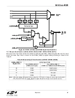
7.7.3. Independent Skew (Si5324, Si5326, Si5368, Si5369, Si5374)
The phase of each clock output may be adjusted in relation to the phase of the other clock outputs, respectively.
This feature is available when
CK_CONFIG_REG
= 0. The resolution of the phase adjustment is equal to [NI HS/
F
VCO
]. Since F
VCO
is approximately 5 GHz and N1_HS = (4, 5, 6, …, 11), the resolution varies from approximately
800 ps to 2.2 ns depending on the PLL divider settings. Silicon Laboratories' PC-based configuration software
(DSPLL
sim
) provides PLL divider settings for each frequency translation, if applicable. If more than one set of PLL
divider settings is available, selecting the combination with the lowest N1_HS value provides the finest resolution
for output clock phase offset control. The
INDEPENDENTSKEWn
[7:0] (n = 1 to 5) register bits control the phase of
the device output clocks. By programming a different phase offset for each output clock, output-to-output delays
can easily be set.
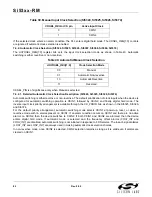
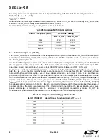
7.7.4. Output-to-output Skew (Si5324, Si5326, Si5327, Si5368, Si5369, Si5374)
The output-to-output skew is guaranteed to be preserved only if the following two register bits are both high:
Register Bit:
Location
CKOUT_ALWAYS_ON
addr 0, bit 5
SQICAL
addr 3, bit 4
In addition, if
SFOUT
is changed, the output-to-output skew may be disturbed until after a successful ICAL.
Note:
CKOUT5 phase is random unless it is used for Frame Sync (See section 7.8).
7.7.5. Input-to-Output Skew (All Devices)
The input-to-output skew for these devices is not controlled.
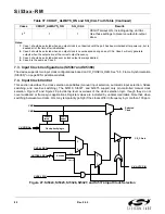
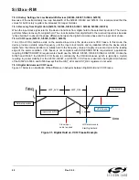
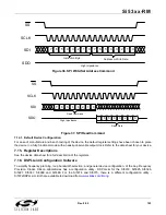
7.8. Frame Synchronization Realignment (Si5368 and CK_CONFIG_REG = 1)
Frame Synchronization Realignment is selected by setting
CK_CONFIG_REG
= 1. In a typical frame
synchronization application, CKIN1 and CKIN2 are high-speed input clocks from primary and secondary clock
generation cards and CKIN3 and CKIN4 are their associated primary and secondary frame synchronization
signals. The device generates four output clocks and a frame sync output FS_OUT. CKIN3 and CKIN4 control the
phase of FS_OUT. When
CK_CONFIG_REG
= 1, the Si5368 can lock onto only CKIN1 or CKIN2. CKIN3 and
CKIN4 are used only for purposes of frame synchronization.
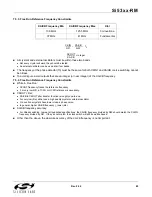
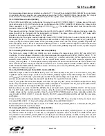
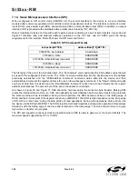
The inputs supplied to CKIN3 and CKIN4 can range from 2 to 512 kHz. So that two different frame sync input
frequencies can be accommodated, CKIN3 and CKIN4 each have their own input dividers, as shown in Figure 32.
The CKIN3 and CKIN4 frequencies are set by the
CKIN3RATE
[2:0] and
CKIN4RATE
[2:0] register bits, as shown in
Table 44. The frequency of FS_OUT can range from 2 kHz to 710 MHz and is set using the NC5_LS divider
setting. FS_OUT must divide evenly into CKOUT2. For example, if CKOUT2 is 156.25 MHz, then 8 kHz would not
be an acceptable frame rate because 156.25 MHz/8 kHz = 19,531.25, which is not an integer. However, 2 kHz
would be an acceptable frame rate because 156.25 MHz/2 kHz = 78,125.
Summary of Contents for Si5316 Series
Page 2: ...Si53xx RM 2 Rev 0 52 ...
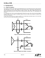
Page 110: ...Si53xx RM 110 Rev 0 52 Figure 48 sfout_5 LVPECL Figure 49 sfout_6 CML ...
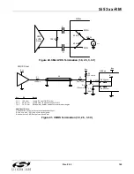
Page 111: ...Si53xx RM Rev 0 52 111 Figure 50 sfout_7 LVDS ...
Page 127: ...Si53xx RM Rev 0 52 127 Figure 66 155 52 MHz In 622 08 MHz Out Loop BW 7 Hz Si5324 ...
Page 128: ...Si53xx RM 128 Rev 0 52 Figure 67 19 44 MHz In 156 25 MHz Out Loop BW 80 Hz ...
Page 129: ...Si53xx RM Rev 0 52 129 Figure 68 19 44 MHz In 156 25 MHz Out Loop BW 5 Hz Si5324 ...
Page 131: ...Si53xx RM Rev 0 52 131 Figure 70 61 44 MHz In 491 52 MHz Out Loop BW 7 Hz Si5324 ...
Page 132: ...Si53xx RM 132 Rev 0 52 Figure 71 622 08 MHz In 672 16 MHz Out Loop BW 6 9 kHz ...
Page 133: ...Si53xx RM Rev 0 52 133 Figure 72 622 08 MHz In 672 16 MHz Out Loop BW 100 Hz ...
Page 134: ...Si53xx RM 134 Rev 0 52 Figure 73 156 25 MHz In 155 52 MHz Out ...
Page 139: ...Si53xx RM Rev 0 52 139 Figure 78 86 685 MHz In 173 371 MHz Out ...
Page 140: ...Si53xx RM 140 Rev 0 52 Figure 79 86 685 MHz In 693 493 MHz Out ...
Page 142: ...Si53xx RM 142 Rev 0 52 Figure 81 10 MHz In 1 GHz Out ...
Page 174: ...Si53xx RM 174 Rev 0 52 Figure 99 Si5374 Si5375 DSPLL A ...
Page 175: ...Si53xx RM Rev 0 52 175 Figure 100 Si5374 Si5375 DSPLL B ...
Page 176: ...Si53xx RM 176 Rev 0 52 Figure 101 Si5374 Si5375 DSPLL C ...


