


S i 5 3 x x - R M
22
Rev. 0.52
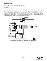
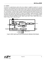
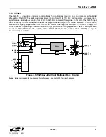
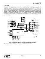
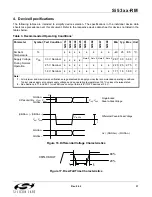
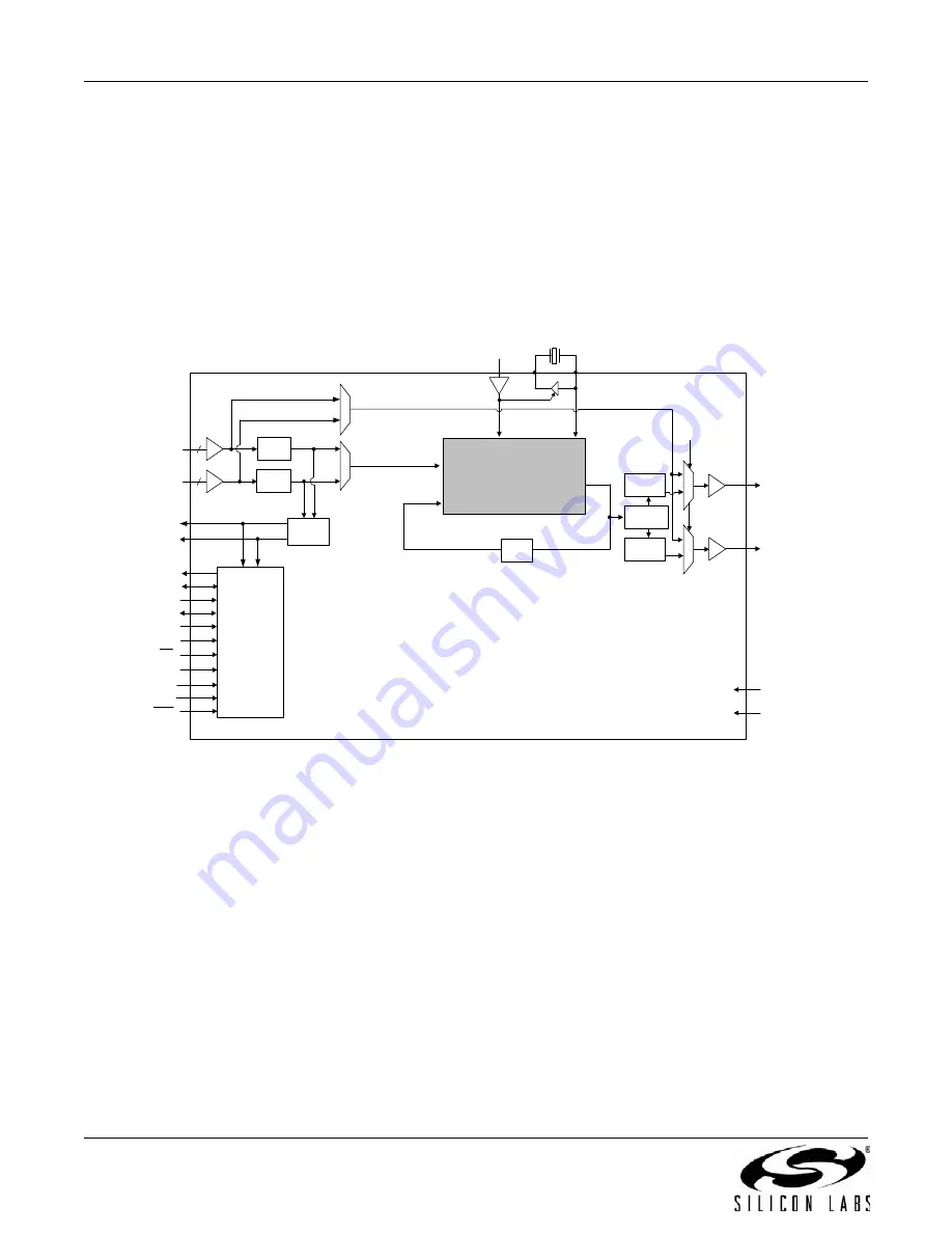
3.7. Si5326
The Si5326 is a jitter-attenuating precision clock multiplier for applications requiring sub 1 ps jitter performance.
The Si5326 accepts dual clock inputs ranging from 2 kHz to 710 MHz and generates two independent,
synchronous clock outputs ranging from 2 kHz to 945 MHz and select frequencies to 1.4 GHz. The device provides
virtually any frequency translation combination across this operating range. The Si5326 input clock frequency and
clock multiplication ratios are programmable through an I
2
C or SPI interface. The DSPLL loop bandwidth is digitally
programmable from 60 Hz to 8 kHz, providing jitter performance optimization at the application level. Operating
from a single 1.8, 2.5, or 3.3 V supply, the Si5326 is ideal for providing clock multiplication and jitter attenuation in
high-performance timing applications. See "7. Microprocessor Controlled Parts (Si5319, Si5324, Si5325, Si5326,
Si5327, Si5367, Si5368, Si5369, Si5374, Si5375)" on page 75 for a complete description.
Figure 7. Si5326 Clock Multiplier and Jitter Attenuator Block Diagram
÷ N31
INT_C1B
Xtal or Refclock
÷ NC1
÷ NC2
Signal
Detect
VDD
GND
C2B
0
1
f
3
C
CKOUT_2 –
C
CKOUT_1 –
/
/
2
2
1
0
1
0
f
OSC
RATE[1:0]
LOL
CS_CA
SDA_SDO
INC
DEC
RST
SCL
Control
SDI
A[2]/SS
A[1:0]
XA
XB
CMODE
CKIN_1 –
2
2
CKIN_2 –
÷ N32
0
1
3
BYPASS
÷ N2
DSPLL
÷ N1_HS
DSPLL
®
Summary of Contents for Si5316 Series
Page 2: ...Si53xx RM 2 Rev 0 52 ...
Page 110: ...Si53xx RM 110 Rev 0 52 Figure 48 sfout_5 LVPECL Figure 49 sfout_6 CML ...
Page 111: ...Si53xx RM Rev 0 52 111 Figure 50 sfout_7 LVDS ...
Page 127: ...Si53xx RM Rev 0 52 127 Figure 66 155 52 MHz In 622 08 MHz Out Loop BW 7 Hz Si5324 ...
Page 128: ...Si53xx RM 128 Rev 0 52 Figure 67 19 44 MHz In 156 25 MHz Out Loop BW 80 Hz ...
Page 129: ...Si53xx RM Rev 0 52 129 Figure 68 19 44 MHz In 156 25 MHz Out Loop BW 5 Hz Si5324 ...
Page 131: ...Si53xx RM Rev 0 52 131 Figure 70 61 44 MHz In 491 52 MHz Out Loop BW 7 Hz Si5324 ...
Page 132: ...Si53xx RM 132 Rev 0 52 Figure 71 622 08 MHz In 672 16 MHz Out Loop BW 6 9 kHz ...
Page 133: ...Si53xx RM Rev 0 52 133 Figure 72 622 08 MHz In 672 16 MHz Out Loop BW 100 Hz ...
Page 134: ...Si53xx RM 134 Rev 0 52 Figure 73 156 25 MHz In 155 52 MHz Out ...
Page 139: ...Si53xx RM Rev 0 52 139 Figure 78 86 685 MHz In 173 371 MHz Out ...
Page 140: ...Si53xx RM 140 Rev 0 52 Figure 79 86 685 MHz In 693 493 MHz Out ...
Page 142: ...Si53xx RM 142 Rev 0 52 Figure 81 10 MHz In 1 GHz Out ...
Page 174: ...Si53xx RM 174 Rev 0 52 Figure 99 Si5374 Si5375 DSPLL A ...
Page 175: ...Si53xx RM Rev 0 52 175 Figure 100 Si5374 Si5375 DSPLL B ...
Page 176: ...Si53xx RM 176 Rev 0 52 Figure 101 Si5374 Si5375 DSPLL C ...


