
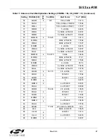


S i 5 3 x x - R M
66
Rev. 0.52
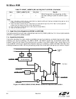
6.3. Pin Control Input Clock Control
This section describes the clock selection capabilities (manual input selection, automatic input selection, hitless
switching, and revertive switching). When switching between two clocks, LOL may temporarily go high if the two
clocks differ in frequency by more than 100 ppm.
6.3.1. Manual Clock Selection
Manual control of input clock selection is chosen via the CS[1:0] pins according to Table 22 and Table 23.
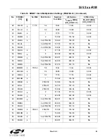
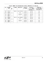
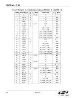
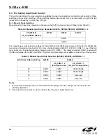
The manual input clock selection settings for the Si5365 and the Si5366 are shown in Table 23. The Si5366 has
two modes of operation (See Section “6.5. Frame Synchronization (Si5366)”). With CK_CONF = 0, any of the four
input clocks may be selected manually; however, when CK_CONF = 1 the inputs are paired, CKIN1 is paired with
CKIN3 and likewise for CKIN2 and CKIN4. Therefore, only two settings are available to select one of the two pairs.
Notes
:
1. To avoid clock switching based on intermediate states during a CS state change, the CS input pins are
internally deglitched.
2. If the selected clock enters an alarm condition, the PLL enters digital hold mode.
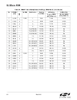
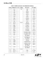
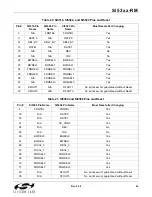
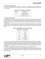
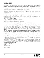
Table 22. Manual Input Clock Selection (Si5316, Si5322, Si5323), AUTOSEL = L
CS (Si5316)
CS_CA (Si5322, Si5323)
Si5316
Si5322
Si5323
0
CKIN1
1
CKIN2
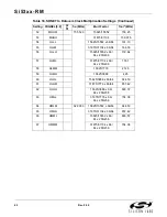
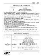
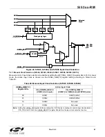
Table 23. Manual Input Clock Selection (Si5365, Si5366), AUTOSEL = L
[CS1_CA4, CS0_CA3]_Pins
Si5365
Si5366
CK_CONF = 0
(5 Output Clocks)
CK_CONF = 1
(FS_OUT Configuration)
00
CKIN1
CKIN1
CKIN1/CKIN3
01
CKIN2
CKIN2
CKIN2/CKIN4
10
CKIN3
CKIN3
Reserved
11
CKIN4
CKIN4
Reserved
Summary of Contents for Si5316 Series
Page 2: ...Si53xx RM 2 Rev 0 52 ...
Page 110: ...Si53xx RM 110 Rev 0 52 Figure 48 sfout_5 LVPECL Figure 49 sfout_6 CML ...
Page 111: ...Si53xx RM Rev 0 52 111 Figure 50 sfout_7 LVDS ...
Page 127: ...Si53xx RM Rev 0 52 127 Figure 66 155 52 MHz In 622 08 MHz Out Loop BW 7 Hz Si5324 ...
Page 128: ...Si53xx RM 128 Rev 0 52 Figure 67 19 44 MHz In 156 25 MHz Out Loop BW 80 Hz ...
Page 129: ...Si53xx RM Rev 0 52 129 Figure 68 19 44 MHz In 156 25 MHz Out Loop BW 5 Hz Si5324 ...
Page 131: ...Si53xx RM Rev 0 52 131 Figure 70 61 44 MHz In 491 52 MHz Out Loop BW 7 Hz Si5324 ...
Page 132: ...Si53xx RM 132 Rev 0 52 Figure 71 622 08 MHz In 672 16 MHz Out Loop BW 6 9 kHz ...
Page 133: ...Si53xx RM Rev 0 52 133 Figure 72 622 08 MHz In 672 16 MHz Out Loop BW 100 Hz ...
Page 134: ...Si53xx RM 134 Rev 0 52 Figure 73 156 25 MHz In 155 52 MHz Out ...
Page 139: ...Si53xx RM Rev 0 52 139 Figure 78 86 685 MHz In 173 371 MHz Out ...
Page 140: ...Si53xx RM 140 Rev 0 52 Figure 79 86 685 MHz In 693 493 MHz Out ...
Page 142: ...Si53xx RM 142 Rev 0 52 Figure 81 10 MHz In 1 GHz Out ...
Page 174: ...Si53xx RM 174 Rev 0 52 Figure 99 Si5374 Si5375 DSPLL A ...
Page 175: ...Si53xx RM Rev 0 52 175 Figure 100 Si5374 Si5375 DSPLL B ...
Page 176: ...Si53xx RM 176 Rev 0 52 Figure 101 Si5374 Si5375 DSPLL C ...


