


S i 5 3 x x - R M
164
Rev. 0.52
A
PPENDIX
H—J
ITTER
A
TTENUATION
AND
L
OOP
BW
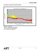
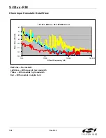
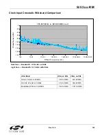
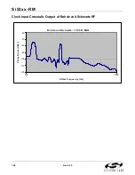
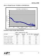
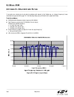
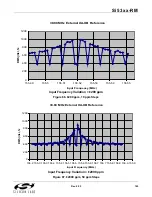
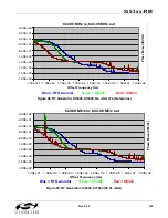
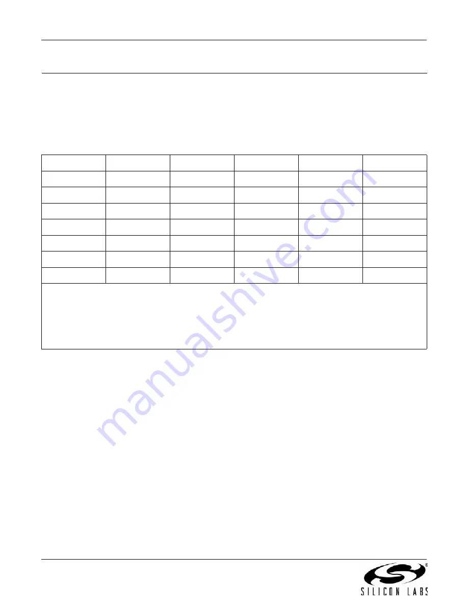
The following illustrates the effects of different loop BW values on the jitter attenuation of the Any-Frequency
devices. The jitter consists of sine wave modulation at varying frequencies. The RMS jitter values of the modulated
sine wave input is compared to the output jitter of an Si5326 and an Si5324. For reference, the top entry in the
table lists the jitter without any modulation. For each entry in the table, the corresponding phase noise plots are
presented.
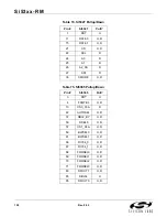
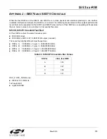
Table 82. Jitter Values
Fmod
Fdev
Jitter Start
RF Gen
Si5326
Si5324
0
0
500 Hz
1.18 ps
283 fs
281 fs
50 Hz
50 Hz
10 Hz
181 ps
169 ps
10.6 ps
100 Hz
100 Hz
50 Hz
177 ps
136 ps
2.04 ps
500 Hz
500 Hz
100 Hz
175 ps
18.6 ps
295 fs
1 kHz
1 kHz
500 Hz
184 ps
4.28 ps
292 fs
5 kHz
5 kHz
500 Hz
138 ps
297 fs
302 fs
10 kHz
10 kHz
500 Hz
139 ps
302 fs
304 fs
Notes:
1.
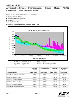
All phase noise plots are with 622.08 MHz input and 622.08 MHz output.
Si5326 bandwidth = 120 Hz; Si5324 bandwidth = 7 Hz.
2.
FM modulation at F = Fmod with modulation amplitude = Fdev.
3.
Jit start is the start of the brick wall integration band. All integration bands end at 50 MHz.
4.
Phase noise measured by Agilent model E5052B.
5.
RF Generator was Rohde and Schwarz model SML03.
Summary of Contents for Si5316 Series
Page 2: ...Si53xx RM 2 Rev 0 52 ...
Page 110: ...Si53xx RM 110 Rev 0 52 Figure 48 sfout_5 LVPECL Figure 49 sfout_6 CML ...
Page 111: ...Si53xx RM Rev 0 52 111 Figure 50 sfout_7 LVDS ...
Page 127: ...Si53xx RM Rev 0 52 127 Figure 66 155 52 MHz In 622 08 MHz Out Loop BW 7 Hz Si5324 ...
Page 128: ...Si53xx RM 128 Rev 0 52 Figure 67 19 44 MHz In 156 25 MHz Out Loop BW 80 Hz ...
Page 129: ...Si53xx RM Rev 0 52 129 Figure 68 19 44 MHz In 156 25 MHz Out Loop BW 5 Hz Si5324 ...
Page 131: ...Si53xx RM Rev 0 52 131 Figure 70 61 44 MHz In 491 52 MHz Out Loop BW 7 Hz Si5324 ...
Page 132: ...Si53xx RM 132 Rev 0 52 Figure 71 622 08 MHz In 672 16 MHz Out Loop BW 6 9 kHz ...
Page 133: ...Si53xx RM Rev 0 52 133 Figure 72 622 08 MHz In 672 16 MHz Out Loop BW 100 Hz ...
Page 134: ...Si53xx RM 134 Rev 0 52 Figure 73 156 25 MHz In 155 52 MHz Out ...
Page 139: ...Si53xx RM Rev 0 52 139 Figure 78 86 685 MHz In 173 371 MHz Out ...
Page 140: ...Si53xx RM 140 Rev 0 52 Figure 79 86 685 MHz In 693 493 MHz Out ...
Page 142: ...Si53xx RM 142 Rev 0 52 Figure 81 10 MHz In 1 GHz Out ...
Page 174: ...Si53xx RM 174 Rev 0 52 Figure 99 Si5374 Si5375 DSPLL A ...
Page 175: ...Si53xx RM Rev 0 52 175 Figure 100 Si5374 Si5375 DSPLL B ...
Page 176: ...Si53xx RM 176 Rev 0 52 Figure 101 Si5374 Si5375 DSPLL C ...


