


Si53xx-RM
Rev. 0.52
101
7.13. I
2
C Serial Microprocessor Interface
When configured in I
2
C control mode (CMODE = L), the control interface to the device is a 2-wire bus for
bidirectional communication. The bus consists of a bidirectional serial data line (SDA) and a serial clock input
(SCL). Both lines must be connected to the positive supply via an external pull-up. In addition, an output interrupt
(INT) is provided with selectable active polarity (determined by
INT_POL
bit). Fast mode operation is supported for
transfer rates up to 400 kbps as specified in the I
2
C-Bus Specification standard. To provide bus address flexibility,
three pins (A[2:0]) are available to customize the LSBs of the device address. The complete bus address for the
device is as follows:
1 1 0 1 A[2] A[1] A[0] R/W.
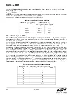
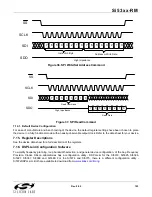
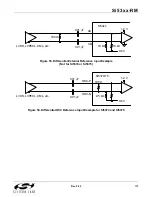
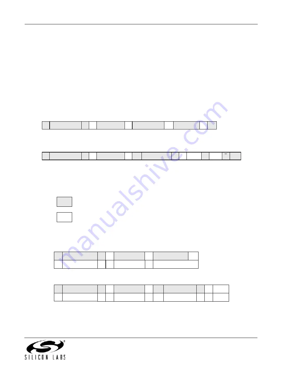
Figure 34 shows the command format for both read and write access. Data is always sent MSB first. The timing
specifications and timing diagram for the I
2
C bus can be found in the I
2
C-Bus Specification standard (fast mode
operation) (See:
http://www.standardics.nxp.com/literature/books/i2c/pdf/i2c.bus.specification.pdf
).
The maximum I
2
C clock speed is 400 kHz.
Figure 34. I
2
C Command Format
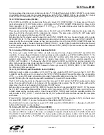
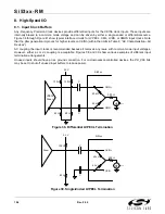
In Figure 35, the value 68 is seven bits. The sequence of the example is: Write register 00 with the value 0xAA;
then, read register 00. Note that 0 = Write = W, and 1 = Read = R.
Figure 35. I
2
C Example
A
Data
A
Data
P
A
1
Slave Address
S
A
Byte
Address
A
0
Slave Address
S
A
Data
A
Data
P
1
Slave Address
S
A
Byte
Address
A
0
Slave Address
S
From master to slave
From slave to master
A – Acknowledge (SDA LOW)
S
– START condition
P – STOP condition
Write Command
Read Command
–address auto incremented after each data read or write
(this can be two separate transactions)
P
A
Data
A
Data
A
Byte
Address
A
0
Slave Address
S
P
A
Data
A
Data
A
Byte
Address
A
0
Slave Address
S
A
Data
1
Slave Address
S
A
Byte Address
A
0
Slave Address
S
Data
0
Write Command
Read Command
A
Data
A
Byte Address
A
0
Slave Address
S
68
W
00
68
R
AA
68
W
00
AA
Summary of Contents for Si5316 Series
Page 2: ...Si53xx RM 2 Rev 0 52 ...
Page 110: ...Si53xx RM 110 Rev 0 52 Figure 48 sfout_5 LVPECL Figure 49 sfout_6 CML ...
Page 111: ...Si53xx RM Rev 0 52 111 Figure 50 sfout_7 LVDS ...
Page 127: ...Si53xx RM Rev 0 52 127 Figure 66 155 52 MHz In 622 08 MHz Out Loop BW 7 Hz Si5324 ...
Page 128: ...Si53xx RM 128 Rev 0 52 Figure 67 19 44 MHz In 156 25 MHz Out Loop BW 80 Hz ...
Page 129: ...Si53xx RM Rev 0 52 129 Figure 68 19 44 MHz In 156 25 MHz Out Loop BW 5 Hz Si5324 ...
Page 131: ...Si53xx RM Rev 0 52 131 Figure 70 61 44 MHz In 491 52 MHz Out Loop BW 7 Hz Si5324 ...
Page 132: ...Si53xx RM 132 Rev 0 52 Figure 71 622 08 MHz In 672 16 MHz Out Loop BW 6 9 kHz ...
Page 133: ...Si53xx RM Rev 0 52 133 Figure 72 622 08 MHz In 672 16 MHz Out Loop BW 100 Hz ...
Page 134: ...Si53xx RM 134 Rev 0 52 Figure 73 156 25 MHz In 155 52 MHz Out ...
Page 139: ...Si53xx RM Rev 0 52 139 Figure 78 86 685 MHz In 173 371 MHz Out ...
Page 140: ...Si53xx RM 140 Rev 0 52 Figure 79 86 685 MHz In 693 493 MHz Out ...
Page 142: ...Si53xx RM 142 Rev 0 52 Figure 81 10 MHz In 1 GHz Out ...
Page 174: ...Si53xx RM 174 Rev 0 52 Figure 99 Si5374 Si5375 DSPLL A ...
Page 175: ...Si53xx RM Rev 0 52 175 Figure 100 Si5374 Si5375 DSPLL B ...
Page 176: ...Si53xx RM 176 Rev 0 52 Figure 101 Si5374 Si5375 DSPLL C ...


