


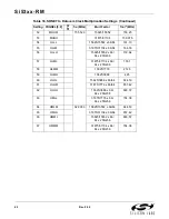

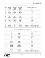
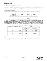


Si53xx-RM
Rev. 0.52
69
6.4. Digital Hold/VCO Freeze
All Any-Frequency Precision Clock devices feature a hold over or VCO freeze mode, whereby the DSPLL is locked
to a digital value.
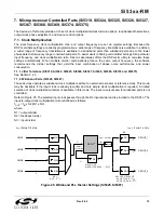
6.4.1. Narrowband Digital Hold (Si5316, Si5323, Si5366)
If an LOS or FOS condition exists on the selected input clock, the device enters digital hold. In this mode, the
device provides a stable output frequency until the input clock returns and is validated. When the device enters
digital hold, the internal oscillator is initially held to its last frequency value. Next, the internal oscillator slowly
transitions to a historical average frequency value that was taken over a time window of 6,711 ms in size that
ended 26 ms before the device entered digital hold. This frequency value is taken from an internal memory location
that keeps a record of previous DSPLL frequency values. By using a historical average frequency, input clock
phase and frequency transients that may occur immediately preceding loss of clock or any event causing digital
hold do not affect the digital hold frequency. Also, noise related to input clock jitter or internal PLL jitter is
minimized.
If a highly stable reference, such as an oven-controlled crystal oscillator, is supplied at XA/XB, an extremely stable
digital hold can be achieved. If a crystal is supplied at the XA/XB port, the digital hold stability will be limited by the
stability of the crystal.
6.4.2. Recovery from Digital Hold (Si5316, Si5323, Si5366)
When the input clock signal returns, the device transitions from digital hold to the selected input clock. The device
performs hitless recovery from digital hold. The clock transition from digital hold to the returned input clock includes
“phase buildout” to absorb the phase difference between the digital hold clock phase and the input clock phase.
6.4.3. Wideband VCO Freeze (Si5322, Si5365)
If an LOS condition exists on the selected input clock, the device freezes the VCO. In this mode, the device
provides a stable output frequency until the input clock returns and is validated. When the device enters VCO
freeze, the internal oscillator is initially held to its last frequency value.
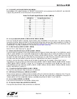
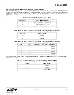
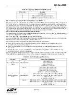
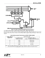
6.5. Frame Synchronization (Si5366)
FSYNC is used in applications that require a synchronizing pulse that has an exact number of periods of a high-
rate clock, Frame Synchronization is selected by setting CK_CONF = 1 and FRQTBL = L). In a typical frame
synchronization application, CKIN1 and CKIN2 are high-speed input clocks from primary and secondary clock
generation cards and CKIN3 and CKIN4 are their associated primary and secondary frame synchronization
signals. The device generates four output clocks and a frame sync output FS_OUT. CKIN3 and CKIN4 control the
phase of FS_OUT.
The frame sync inputs supplied to CKIN3 and CKIN4 must be 8 kHz. Since the frequency of FS_OUT is derived
from CKOUT2, CKOUT2 must be a standard SONET frequency (e.g. 19.44 MHz, 77.76 MHz). Table 16 lists the
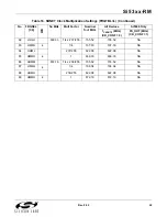
input frequency/clock multiplication ratio combinations supporting an 8 kHz output on FS_OUT.
Summary of Contents for Si5316 Series
Page 2: ...Si53xx RM 2 Rev 0 52 ...
Page 110: ...Si53xx RM 110 Rev 0 52 Figure 48 sfout_5 LVPECL Figure 49 sfout_6 CML ...
Page 111: ...Si53xx RM Rev 0 52 111 Figure 50 sfout_7 LVDS ...
Page 127: ...Si53xx RM Rev 0 52 127 Figure 66 155 52 MHz In 622 08 MHz Out Loop BW 7 Hz Si5324 ...
Page 128: ...Si53xx RM 128 Rev 0 52 Figure 67 19 44 MHz In 156 25 MHz Out Loop BW 80 Hz ...
Page 129: ...Si53xx RM Rev 0 52 129 Figure 68 19 44 MHz In 156 25 MHz Out Loop BW 5 Hz Si5324 ...
Page 131: ...Si53xx RM Rev 0 52 131 Figure 70 61 44 MHz In 491 52 MHz Out Loop BW 7 Hz Si5324 ...
Page 132: ...Si53xx RM 132 Rev 0 52 Figure 71 622 08 MHz In 672 16 MHz Out Loop BW 6 9 kHz ...
Page 133: ...Si53xx RM Rev 0 52 133 Figure 72 622 08 MHz In 672 16 MHz Out Loop BW 100 Hz ...
Page 134: ...Si53xx RM 134 Rev 0 52 Figure 73 156 25 MHz In 155 52 MHz Out ...
Page 139: ...Si53xx RM Rev 0 52 139 Figure 78 86 685 MHz In 173 371 MHz Out ...
Page 140: ...Si53xx RM 140 Rev 0 52 Figure 79 86 685 MHz In 693 493 MHz Out ...
Page 142: ...Si53xx RM 142 Rev 0 52 Figure 81 10 MHz In 1 GHz Out ...
Page 174: ...Si53xx RM 174 Rev 0 52 Figure 99 Si5374 Si5375 DSPLL A ...
Page 175: ...Si53xx RM Rev 0 52 175 Figure 100 Si5374 Si5375 DSPLL B ...
Page 176: ...Si53xx RM 176 Rev 0 52 Figure 101 Si5374 Si5375 DSPLL C ...


