


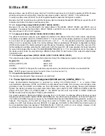

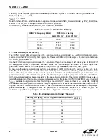
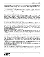


S i 5 3 x x - R M
84
Rev. 0.52
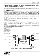
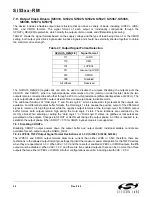
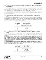
7.5. Si5319, Si5324, Si5326, Si5327, Si5368, Si5369, Si5374 and Si5375 Free Run Mode
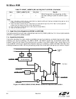
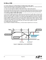
Figure 29. Free Run Mode Block Diagram
CKIN2 has an extra mux with a path to the crystal oscillator output.
When in Free Run mode, CKIN2 is sacrificed (Si5326, Si5368, Si5369, Si5374).
Switching between the crystal oscillator and CLKIN1 is hitless.
Either a crystal or an external oscillator can be used.
External oscillator connection can be either single ended or differential.
All other features and specifications remain the same.
7.5.1. Free Run Mode Programming Procedure
Using DSPLL
sim
, determine the frequency plan:
Write to the internal dividers, including N31 and N32.
Enable Free Run Mode (the mux select line),
FREE_RUN
.
Select CKIN1 as the higher priority clock.
Establish revertive and autoselect modes.
Once properly programmed, the part will:
Initially lock to either the XA/XB (OSC_P and OSC_N for the Si5374/75) or to CKIN1.
Automatically select CKIN1, if it is available.
Automatically and hitlessly switch to XA/XB if CKIN1 fails.
Automatically and hitlessly switch back to CKIN1 when it subsequently returns.
For the Si5319:
Clock selection is manual using an input pin.
Clock switching is not hitless.
CKIN2 is not available.
7.5.2. Clock Control Logic in Free Run Mode
Noting that the mux that selects CKIN2 versus the XA/XB oscillator is located before the clock selection and control
logic, when in Free Run mode operation, all such logic will be driven by the XA/XB oscillator, not the CKIN2 pins.
For example, when in Free Run mode, the CK2B pin will reflect the status of the XA/XB oscillator and not the status
of the CKIN2 pins.
C rystal or an external oscillator
(external oscillator only for the Si5374/75)
S i5319,
S i5324,
S i5326,
S i5327,
S i5368,
S i5369,
S i5374,
S i5375
C K O U T1
C K O U T2
X tal osc
D S P LL
C ore
C K IN 1
I
2
C /S P I
C K IN 2
C ontrol
X A -X B
N 31
N 31
N 32
N 32
XA
X B
Summary of Contents for Si5316 Series
Page 2: ...Si53xx RM 2 Rev 0 52 ...
Page 110: ...Si53xx RM 110 Rev 0 52 Figure 48 sfout_5 LVPECL Figure 49 sfout_6 CML ...
Page 111: ...Si53xx RM Rev 0 52 111 Figure 50 sfout_7 LVDS ...
Page 127: ...Si53xx RM Rev 0 52 127 Figure 66 155 52 MHz In 622 08 MHz Out Loop BW 7 Hz Si5324 ...
Page 128: ...Si53xx RM 128 Rev 0 52 Figure 67 19 44 MHz In 156 25 MHz Out Loop BW 80 Hz ...
Page 129: ...Si53xx RM Rev 0 52 129 Figure 68 19 44 MHz In 156 25 MHz Out Loop BW 5 Hz Si5324 ...
Page 131: ...Si53xx RM Rev 0 52 131 Figure 70 61 44 MHz In 491 52 MHz Out Loop BW 7 Hz Si5324 ...
Page 132: ...Si53xx RM 132 Rev 0 52 Figure 71 622 08 MHz In 672 16 MHz Out Loop BW 6 9 kHz ...
Page 133: ...Si53xx RM Rev 0 52 133 Figure 72 622 08 MHz In 672 16 MHz Out Loop BW 100 Hz ...
Page 134: ...Si53xx RM 134 Rev 0 52 Figure 73 156 25 MHz In 155 52 MHz Out ...
Page 139: ...Si53xx RM Rev 0 52 139 Figure 78 86 685 MHz In 173 371 MHz Out ...
Page 140: ...Si53xx RM 140 Rev 0 52 Figure 79 86 685 MHz In 693 493 MHz Out ...
Page 142: ...Si53xx RM 142 Rev 0 52 Figure 81 10 MHz In 1 GHz Out ...
Page 174: ...Si53xx RM 174 Rev 0 52 Figure 99 Si5374 Si5375 DSPLL A ...
Page 175: ...Si53xx RM Rev 0 52 175 Figure 100 Si5374 Si5375 DSPLL B ...
Page 176: ...Si53xx RM 176 Rev 0 52 Figure 101 Si5374 Si5375 DSPLL C ...


