


Si53xx-RM
Rev. 0.52
47
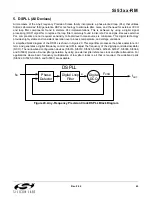
5.2. PLL Performance
All members of the Any-Frequency Precision Clock family of devices provide extremely low jitter generation, a well-
controlled jitter transfer function, and high jitter tolerance. For more information the loop bandwidth and its effect on
jitter attenuation, see "Appendix H—Jitter Attenuation and Loop BW" on page 164.
5.2.1. Jitter Generation
Jitter generation is defined as the amount of jitter produced at the output of the device with a jitter free input clock.
Generated jitter arises from sources within the VCO and other PLL components. Jitter generation is a function of
the PLL bandwidth setting. Higher loop bandwidth settings may result in lower jitter generation, but may result in
less attenuation of jitter that might be present on the input clock signal.
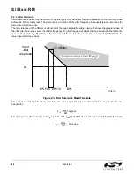
5.2.2. Jitter Transfer
Jitter transfer is defined as the ratio of output signal jitter to input signal jitter for a specified jitter frequency. The
jitter transfer characteristic determines the amount of input clock jitter that passes to the outputs. The DSPLL
technology used in the Any-Frequency Precision Clock devices provides tightly controlled jitter transfer curves
because the PLL gain parameters are determined largely by digital circuits which do not vary over supply voltage,
process, and temperature. In a system application, a well-controlled transfer curve minimizes the output clock jitter
variation from board to board and provides more consistent system level jitter performance.
The jitter transfer characteristic is a function of the loop bandwidth setting. Lower bandwidth settings result in more
jitter attenuation of the incoming clock, but may result in higher jitter generation. Section 1 Any-Frequency
Precision Clock Product Family Overview also includes specifications related to jitter bandwidth and peaking.
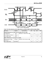
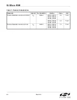
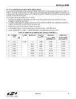
Figure 22 shows the jitter transfer curve mask.
Figure 22. PLL Jitter Transfer Mask/Template
Jitter
Transfer
0 dB
BW
f
Jitter
Peaking
–20 dB/dec.
Jitter Out
Jitter In
)
(
20 x LOG
Summary of Contents for Si5316 Series
Page 2: ...Si53xx RM 2 Rev 0 52 ...
Page 110: ...Si53xx RM 110 Rev 0 52 Figure 48 sfout_5 LVPECL Figure 49 sfout_6 CML ...
Page 111: ...Si53xx RM Rev 0 52 111 Figure 50 sfout_7 LVDS ...
Page 127: ...Si53xx RM Rev 0 52 127 Figure 66 155 52 MHz In 622 08 MHz Out Loop BW 7 Hz Si5324 ...
Page 128: ...Si53xx RM 128 Rev 0 52 Figure 67 19 44 MHz In 156 25 MHz Out Loop BW 80 Hz ...
Page 129: ...Si53xx RM Rev 0 52 129 Figure 68 19 44 MHz In 156 25 MHz Out Loop BW 5 Hz Si5324 ...
Page 131: ...Si53xx RM Rev 0 52 131 Figure 70 61 44 MHz In 491 52 MHz Out Loop BW 7 Hz Si5324 ...
Page 132: ...Si53xx RM 132 Rev 0 52 Figure 71 622 08 MHz In 672 16 MHz Out Loop BW 6 9 kHz ...
Page 133: ...Si53xx RM Rev 0 52 133 Figure 72 622 08 MHz In 672 16 MHz Out Loop BW 100 Hz ...
Page 134: ...Si53xx RM 134 Rev 0 52 Figure 73 156 25 MHz In 155 52 MHz Out ...
Page 139: ...Si53xx RM Rev 0 52 139 Figure 78 86 685 MHz In 173 371 MHz Out ...
Page 140: ...Si53xx RM 140 Rev 0 52 Figure 79 86 685 MHz In 693 493 MHz Out ...
Page 142: ...Si53xx RM 142 Rev 0 52 Figure 81 10 MHz In 1 GHz Out ...
Page 174: ...Si53xx RM 174 Rev 0 52 Figure 99 Si5374 Si5375 DSPLL A ...
Page 175: ...Si53xx RM Rev 0 52 175 Figure 100 Si5374 Si5375 DSPLL B ...
Page 176: ...Si53xx RM 176 Rev 0 52 Figure 101 Si5374 Si5375 DSPLL C ...


