


S i 5 3 x x - R M
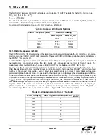
104
Rev. 0.52
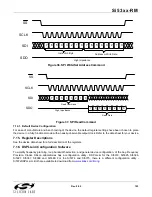
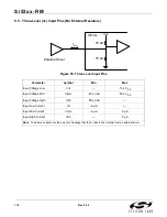
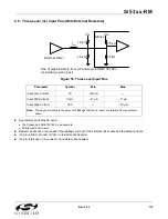
8. High-Speed I/O
8.1. Input Clock Buffers
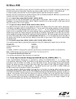
Any-Frequency Precision Clock devices provide differential inputs for the CKINn clock inputs. These inputs are
internally biased to a common mode voltage and can be driven by either a single-ended or differential source.
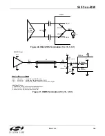
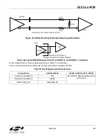
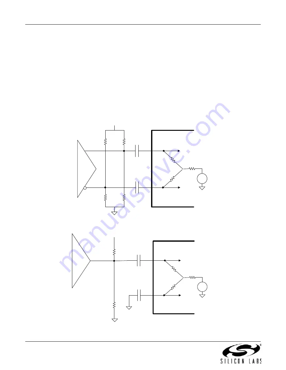
Figure 38 through Figure 41 show typical interface circuits for LVPECL, CML, LVDS, or CMOS input clocks. Note
that the jitter generation improves for higher levels on CKINn (within the limits in Table 8, “AC Characteristics—All
Devices”).
AC coupling the input clocks is recommended because it removes any issue with common mode input voltages.
However, either ac or dc coupling is acceptable. Figures 38 and 39 show various examples of different input
termination arrangements.
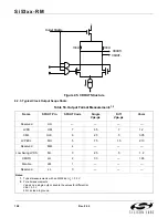
Unused inputs should have an ac ground connection. For microprocessor-controlled devices, the
PD_CKn
bits
may be set to shut off unused input buffers to reduce power.
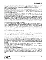
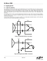
Figure 38. Differential LVPECL Termination
Figure 39. Single-Ended LVPECL Termination
40 k
C
C
±
CKIN
_
CKIN +
V
ICM
300
130
130
3.3 V
82
82
Si53xx
LVPECL
Driver
40 k
40 k
C
C
±
CKIN
_
CKIN +
V
ICM
300
130
3.3 V
82
Si53xx
Driver
40 k
Summary of Contents for Si5316 Series
Page 2: ...Si53xx RM 2 Rev 0 52 ...
Page 110: ...Si53xx RM 110 Rev 0 52 Figure 48 sfout_5 LVPECL Figure 49 sfout_6 CML ...
Page 111: ...Si53xx RM Rev 0 52 111 Figure 50 sfout_7 LVDS ...
Page 127: ...Si53xx RM Rev 0 52 127 Figure 66 155 52 MHz In 622 08 MHz Out Loop BW 7 Hz Si5324 ...
Page 128: ...Si53xx RM 128 Rev 0 52 Figure 67 19 44 MHz In 156 25 MHz Out Loop BW 80 Hz ...
Page 129: ...Si53xx RM Rev 0 52 129 Figure 68 19 44 MHz In 156 25 MHz Out Loop BW 5 Hz Si5324 ...
Page 131: ...Si53xx RM Rev 0 52 131 Figure 70 61 44 MHz In 491 52 MHz Out Loop BW 7 Hz Si5324 ...
Page 132: ...Si53xx RM 132 Rev 0 52 Figure 71 622 08 MHz In 672 16 MHz Out Loop BW 6 9 kHz ...
Page 133: ...Si53xx RM Rev 0 52 133 Figure 72 622 08 MHz In 672 16 MHz Out Loop BW 100 Hz ...
Page 134: ...Si53xx RM 134 Rev 0 52 Figure 73 156 25 MHz In 155 52 MHz Out ...
Page 139: ...Si53xx RM Rev 0 52 139 Figure 78 86 685 MHz In 173 371 MHz Out ...
Page 140: ...Si53xx RM 140 Rev 0 52 Figure 79 86 685 MHz In 693 493 MHz Out ...
Page 142: ...Si53xx RM 142 Rev 0 52 Figure 81 10 MHz In 1 GHz Out ...
Page 174: ...Si53xx RM 174 Rev 0 52 Figure 99 Si5374 Si5375 DSPLL A ...
Page 175: ...Si53xx RM Rev 0 52 175 Figure 100 Si5374 Si5375 DSPLL B ...
Page 176: ...Si53xx RM 176 Rev 0 52 Figure 101 Si5374 Si5375 DSPLL C ...


