background image

Circuit Description

Samsung Electronics

13-25

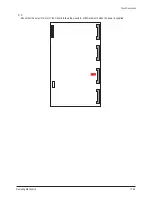
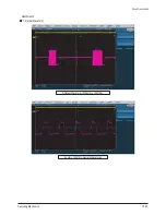
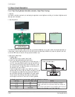
3) X

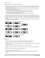
- Check that the output of X-Out of the X board follows the waveform of #Attachment 2 when the power is supplied.

XOUT

Summary of Contents for HP-R5052

Page 1: ...AY TV FEATURES NTSC ATSC Tuner Built In 12 Bit Processing 68 7 Billion Colors Split Screen Picture In Picture Samsung DNIe Digital Natural Image engine SRS TruSurround XT 1 HDMI Input Energy Saving Anynet System Control Solution SAMSUNG EPG System Digital Cable Card Slot SERVICE Manual HP R5052 ...

Page 2: ...l is a property of Samsung Electronics Co Ltd Any unauthorized use of Manual can be punished under applicable International and or domestic law Samsung Electronics Co Ltd Jul 2005 Printed in Korea AA82 02311A ELECTRONICS ...

Page 3: ... Service Mode 3 2 3 3 Factory Data 3 3 3 4 Service Adjustment 3 11 3 5 Software Upgrade 3 16 3 6 Replacements Calibration 3 18 Chapter 4 Exploded View Part List 4 1 HPR5052X XAA 4 1 Chapter 5 Electrical Part List 5 1 HPR5052X XAA Service Item 5 1 Chapter 6 Troubleshooting 6 1 First Checklist for Troubleshooting 6 1 6 2 Checkpoints by Error Mode 6 2 6 3 Troubleshooting Procedures by ASS Y 6 7 Chapt...

Page 4: ...TUNER 10 1 10 2 SOUND PROCESS 10 2 10 3 MICOM IO EX AV IN OUT 10 3 10 4 HDMI PC 10 4 10 5 SVP EX52 10 5 10 6 S3C2800 10 6 10 7 EAGLE 10 7 10 8 POD 10 8 10 9 DNIe Lite LVDS 10 9 10 10 Function A ssy Board 10 10 10 11 Power IR A ssy Board 10 11 ...

Page 5: ...AY TV FEATURES NTSC ATSC Tuner Built In 12 Bit Processing 68 7 Billion Colors Split Screen Picture In Picture Samsung DNIe Digital Natural Image engine SRS TruSurround XT 1 HDMI Input Energy Saving Anynet System Control Solution SAMSUNG EPG System Digital Cable Card Slot SERVICE Manual HP R5052 ...

Page 6: ...l is a property of Samsung Electronics Co Ltd Any unauthorized use of Manual can be punished under applicable International and or domestic law Samsung Electronics Co Ltd Jul 2005 Printed in Korea AA82 02311A ELECTRONICS ...

Page 7: ... Service Mode 3 2 3 3 Factory Data 3 3 3 4 Service Adjustment 3 11 3 5 Software Upgrade 3 16 3 6 Replacements Calibration 3 18 Chapter 4 Exploded View Part List 4 1 HPR5052X XAA 4 1 Chapter 5 Electrical Part List 5 1 HPR5052X XAA Service Item 5 1 Chapter 6 Troubleshooting 6 1 First Checklist for Troubleshooting 6 1 6 2 Checkpoints by Error Mode 6 2 6 3 Troubleshooting Procedures by ASS Y 6 7 Chapt...

Page 8: ...hapter 11 Operation Instruction Installation 11 1 Product Features and Functions 11 1 11 2 New Features 11 5 11 3 Installation Notes and Precautions 11 7 Chapter 12 Disassembly Reassembly 12 1 Overhaul Disassembly Reassembly 12 1 Chapter 13 Circuit Description 13 1 Power ON OFF Signal Timing Sequence 13 1 13 2 Partial Block Description 13 2 13 3 New Circuit Description 13 28 Chapter 14 Reference I...

Page 9: ...out insulated transformers the product can only be repaired safely when the chassis is connected to the earthed end of the AC power source To make sure the AC power cord is properly connected follow the instructions below Use the voltmeter to measure the voltage between the chassis and the earthed ground If the measurement is over 1 0V unplug the AC power cord and change the polarity before re ins...

Page 10: ...eplaced with another irregular one the safety or protective features will be lost even if the new one has a higher voltage or more watts Critical safety parts should be bracketed with Use only regular parts for replacements in particular flame resistance and dielectric strength specifications Irregular parts or materials may cause electric shock or fire Precaution 1 2 Samsung Electronics ...

Page 11: ...sistance between the blade of the AC plug and that of the conductive material should be more than 1 7 Any B interlock should not be damaged If the metal heat sink is not properly installed no connection to the AC power should be made 8 Make sure the grounding lead of the tester is connected to the chassis ground before connecting to the positive lead The ground lead of the tester should be removed...

Page 12: ... for soldering purposes 6 Use only anti static solder removal devices Most solder removal devices do not support an anti static feature A solder removal device without an anti static feature can store enough static electricity to cause damage to the ESD 7 Do not remove the ESD from the protective box until the replacement is ready Most ESD replacements are covered with lead which will cause a shor...

Page 13: ...ositioning the product Also check the antenna cable or the external connectors if they are fully unplugged Damage to the cord may cause fire or electric shock 6 Keep the antenna far away from any high voltage cables and install it firmly Contact with the high voltage cable or the antenna falling over may cause fire or electric shock 7 When connecting the RF antenna check for a DTV receiving system...

Page 14: ...1 6 Samsung Electronics MEMO ...

Page 15: ...122 Optical Coaxial Output Cabinet S5 Design New Cabinet Chip Description DNVD355BH401A Tuner ATSC NTSC QAM POD NIM Tuner STP22 Component CVBS Y C HDMI PC input Video signal processor SDP43 The DNIe IC for visual quality improvement DNIe Lite Sii9993 Converts the TMDS signal on the HDMI input into 8 bit digital R G B signals MSP4440G Sound Processing IC MST9883 A D converts the R G B input signal ...

Page 16: ... VIDEO COMPONENT1 480i 480p 720p 1080i COMPONENT2 480i 480p 720p 1080i PC DVI AV Output AUDIO L R Speaker Output 15W 15W 8Ω Audio Output OPTICAL DIGITALOUT COAXIAL DIGITALOUT ETC DNIe Lite Anynet Color Weakness My Color Control SRS TruSurround XT Dolby Digital Built in Speaker Stand POD Cable card slot New Function Energy Saving Screen Burn Protection H W Configuration DTV Module S5H2010A01 MPEG D...

Page 17: ...DTV PCM HDMI Feature Component Interface 480i 480p 720p 1080i Y Pb Pr Digital Interface HDMI 480p 720p 1080i Auto Program Sleep Timer 180 Minutes Anynet Interface My Color Control Color Weakness Energy Saving Screen Burn Protection In Out Terminals 1 Monitor audio Output 2 Component Inputs 15 Pin PC D sub Input 1 HDMI Input 2 SPDIF Output Optical Coaxial 2 RF Input Cable Air 1 CVBS Input 1 S Video...

Page 18: ...rtical Polarity Horizontal Polarity IBM PC AT Compatible 640 X 350 70 086 31 469 P N 720 X 400 70 087 31 469 N P 640 X 480 59 940 31 469 N N 70 000 35 000 N P N P 72 809 37 861 N N 75 000 37 500 N N 800 X 600 56 250 35 156 N P N P 60 317 37 879 P P 70 000 43 75 N P N P 72 188 48 077 P P 75 000 46 875 P P 1024 X 768 60 004 48 363 N N 70 069 56 476 N N 72 000 57 672 N P N P 75 029 60 023 P P 1280 X ...

Page 19: ...nd 103 17 Lbs Without Stand Picture Brightness 1 000 Cd m2 1 000 Cd m2 1 300 Cd m2 Contrast Ratio 3 000 1 3 000 1 10 000 1 Picture Enhacer DNIe 2 DNIe 2 DNIe Lite Comb Filter Audio Equalizer 5 Band 5 Band 5 Band Auto Volume Control Surround Sound SRS TruSurround XT SRS TruSurround XT SRS TruSurround XT Dolby Digital Speaker Output 15W 15W 15W 15W 15W 15W Features PIP Double Window Caption Still Im...

Page 20: ...ons BN68 00835A Samsung Service center Remote Control AAA Batteries BN59 00462A 4301 000103 Power Cord 3903 000144 Anynet Cable BN39 00518A Accessories that can be purchased additionally S VIDEO Cable Internal shopping mall HDMI Cable HDMI DVI cable Component Cables RCA PC Cable PC Audio Cable Optical Cable Coaxial Cable Antenna Cable ...

Page 21: ... Voltage Adjustment ASSY PCB P SMPS DC DC BN96 01856A Voltage Adjustment ASSY PCB P SMPS POD BN96 01805A ASSY PDP P LOGIC BOARD BN96 02031A ASSY PDP P X MAIN BOARD BN96 02024A ASSY PDP P Y MAIN BOARD BN96 02025A ASSY PDP P Y UPPER BUFFER BOARD BN96 02026A ASSY PDP P Y LOWER BUFFER BOARD BN96 02027A ASSY PDP P ADDRESS E BUFF BOARD BN96 02028A ASSY PDP P ADDRESS F BUFF BOARD BN96 02029A ASSY PDP P A...

Page 22: ...MODE DISPLAY State T STRANUS0S 0036 and T STRANUS5 0117 are firmware version The firmware version is subject to change without notice 6 Buttons operations within Service Mode MENU Full Menu Display Move to Parent Menu Direction keys Item Selection by Moving the Cursor Direction keys Data Increase Decrease for the Selected Item Source Cycles through the active input source that are connected to the...

Page 23: ...T VCT Ver Check 0 V Chip Enable 1 Watchdog Enable 1 Spread Enable PC 1 Clock Adjust 4 Nim Version T310 MSP Version G New_WB_CbCr 1 ITEM Range Initial Values of Input Modes TV AV S video Component PC HDMI Sub Bright SVP 0 1204 495 513 480 492 R Offset 0 1204 516 512 512 515 G Offset 0 1204 512 512 512 512 B offset 0 1204 512 512 512 511 Sub Contrast DNIe 0 255 130 131 128 131 R Gain 0 255 128 128 1...

Page 24: ... 0 255 120 120 120 120 02 TCD3 Brightness 0 255 49 49 49 49 03 TCD3 YC Delay 0 15 1 1 1 1 04 Analog Y Offset 0 1023 61 61 61 61 05 Analog PB Offset 0 1023 512 512 512 512 06 Analog PR Offset 0 1023 512 512 512 512 07 Analog Y Gain 0 255 217 217 217 217 08 Analog PB Gain 0 255 225 225 225 225 09 Analog PR Gain 0 255 225 225 225 225 10 Black Level Setting 0 255 16 16 0 16 11 Brightness 0 255 128 125...

Page 25: ... 7 7 7 10 7 7 7 10 PeakTh2 P1 Luma Croma 0x16 7 0 0 255 2 2 2 2 0 3 2 2 2 11 PeakTh3 P1 Luma Croma 0x19 7 0 0 255 32 32 32 32 32 34 32 32 32 12 PeakN1Factor2 P1 Luma Croma 0x14 7 5 P1 Luma Croma 0x13 7 5 0 63 56 8 8 8 0 8 0 0 0 13 PeakN1Factor1 P1 Luma Croma 0x1A 5 0 0 63 40 48 48 40 48 40 40 40 40 14 CoringTh P1 Luma Croma 0x17 7 0 0 255 2 2 2 2 2 2 2 2 2 15 CoringGain P1 Luma Croma 0x18 4 0 0 31...

Page 26: ...le 0 255 0x20 NICAM Prescale 0 255 0x20 AV Prescale 0 255 0x1C I2S_1 Prescale 0 255 0x10 I2S_3 Prescale 0 255 0x11 Carrier Mute 0 255 On Pilot High 0 255 0x0D Pilot Low 0 255 0x07 Scart1 Out Volume 0 255 0x6D Scart2 Out Volume 0 255 0x73 ITEM Range Initial Values of Input Modes TV AV SVHS Component PC HDMI RF PAL B G 0 255 0 RF PAL D K 0 255 0 RF PAL I 0 255 0 RF SECAM B G 0 255 0 RF SECAM D K 0 2...

Page 27: ...9 White Balance Post 1 R Offset Post 512 511 0 0 0 0 2 G Offset Post 512 511 0 0 0 0 3 B Offset Post 512 511 0 0 0 0 4 R Gain Post 0 255 0 128 128 128 5 G Gain Post 0 255 0 128 128 128 6 B Gain Post 0 255 0 128 128 128 7 Com_Offset_Sel 0 1 1 0 0 0 8 Com_Gain_Sel 0 1 1 0 0 0 10 ColorTone Cool2 Refer to Table 3 11 ColorTone Cool1 12 ColorTone Normal 13 ColorTone Warm1 14 ColorTone Warm2 15 MCM_EN 0 ...

Page 28: ...ht 0 0 0 0 09 Standard Color 0 0 0 0 10 Standard Sharpness 0 0 0 0 11 Movie Contrast 12 Movie Bright 13 Movie Color 14 Movie Sharpness 15 RF_dB_1 Rf AV Noise Thres1 0 255 20 20 LowPassGain1 0 31 7 14 BandPassGain1 0 31 12 19 HighPassGain1 0 31 6 16 PeakStep1 1 1 CoringTh1 2 2 CoringGain1 8 2 PosGain1 1 1 NegGain1 1 1 V PosGain1 3 3 V NegGain1 2 2 16 RF_dB_2 Noise Thres2 30 40 LowPassGain2 5 10 Ban...

Page 29: ...10 Test Pattern 01 OSD Pattern 01 Luma Ramp 32 Step 02 Luma Ramp 128 Step 03 White 16 04 White 240 05 Color Bar 06 RGB Ramp 32 Step 07 Cross Hatch 20X20 02 1 Channel Pattern 01 Y Filter 02 V PosGain 03 V NegGain 04 V BpGain 05 V HfGain 06 V Peaking Th1 07 V Peaking Th3 03 2 Channel Pattern 01 Luma Ramp 32 Step 02 Luma Ramp 128 Step 03 White 16 04 White 240 05 Color Bar 06 RGB Ramp 32 Step 07 Cross...

Page 30: ... Line Range 0 1 1 02 Sound SD delay 0 2 1 03 Sound HD delay 0 2 1 04 Sound DTV delay 0 1 0 05 DDC Write 0 1 0 06 Auto Voltage Adj 5 07 Image Sticking 0 08 Error Mode Check 1 09 Error Code Table 4 10 Patt Sel 0 11 Control Key Lock 0 12 FCRL Con 1 13 Option PDP ON OFF 14 Reset Factory reset User settings in OSD is initialized ...

Page 31: ...L pattern Use other equipment only after comparing the result with that of the Master equipment Set Aging Time Longer than 30 min Pattern Resolution Given below Calibration Available None and Pattern used for Calibration White Balance coordinates configuration result On the basis of the ABL pattern The resolutions are given below For PC Mode perform only calibration and do not perform additional W...

Page 32: ... 128 128 G Gain 128 128 128 128 128 B gain 128 128 128 128 128 R Cutoff 128 128 128 128 128 G Cutoff 128 128 128 128 128 B Cutoff 128 128 128 128 128 PC R Gain 128 128 128 128 128 G Gain 128 128 128 128 128 B gain 128 128 128 128 128 R Cutoff 128 128 128 128 128 G Cutoff 128 128 128 128 128 B Cutoff 128 128 128 128 128 R Gain 128 128 128 128 128 G Gain 128 128 128 128 128 B gain 128 128 128 128 12...

Page 33: ...gnal to the VIDEO IN port 3 Press the Source key to switch to AV S VIDEO mode 4 After confirming that the Lattice pattern appears select the Calibration menu 5 Select the AV Calibration menu 6 In AV Calibration Off status press the key to perform Calibration 7 When Calibration is complete it returns to the high level menu 8 Apply the 720p Lattice No 6 pattern signal to the COMPONENT IN Y Pb Pr por...

Page 34: ...m the data c Adjust the low light Refer to Picture 2 3 for measurement point Adjust Sub Bright SVP to set the Y value Adjust red offset x and blue offset y to the color coordinates Do not adjust green offset data d Adjust the high light Refer to Picture 2 4 for measurement point Adjust Sub Contrast DNIe to set the Y value Adjust red gain x and blue gain y to the color coordinates Do not adjust the...

Page 35: ...ust white balance with 10 steps gray scale pattern of Picture 2 5 2 When you measure Low Light use 20 IRE portions And When you measure High Light use 70 IRE portion But if color noise is less in 60 IRE than in 70 IRE 60 IRE is allowed as a measure point 3 Perform adjustments 2 b through 2 d from previous page using the 10 step gray scale pattern Picture 2 5 ...

Page 36: ...RS 232 serial port and downloaded file If you want to change serial port you must edit bootdn bat and appdn bat bootdn bat sdn 1 0xdeadbbbb rom execution file file to be downloaded port number downloading type boot image appdn bat sdn 1 0xdeadaaaa ram z execution file file to be downloaded port number downloading type application image 1 Don t turn off during downloading 2 sdn exe download file an...

Page 37: ...reen Place the cursor over the On of Function Help and press the Info key on the remote control The version of the program is displayed at the bottom of the Menu screen 2 Procedures for checking in the Factory Menu When entering Factory Mode the version of the software is displayed at the bottom of the menu as described on page 3 2 Main Program Version Boot code Version ...

Page 38: ...l voltages must be adjusted after changing SMPS PCB or PDP module Range Board Adjustment Vs 190 220V SMPS MAIN Va 60 80V Vset 180 210V SMPS DC DC Ve 80 120V Vscan 160 210V Voltage Label SMPS POD SMPS MAIN SMPS DC DC 2 A point of adjusting SMPS MAIN voltage TP Vs TOP Va BOT Va Adjustment Point Vs Adjustment Point ...

Page 39: ...Alignment Adjustment Samsung Electronics 3 19 3 A point of adjusting SMPS DC DC Use base chassis of PDP panel as GND point ...

Page 40: ...3 20 Samsung Electronics MEMO ...

Page 41: ...A ASSY BOARD P FUNCTION SCHUBERT CT5000 32 1 S A M0146 BN96 02050B ASSY BOARD P POWER IR SCHUBERT CT5000 1 S N A T0003 BN96 01787C ASSY COVER P FRONT 50P5 50S5 EXPORT 1 S A T0023 BN64 00336A KNOB POWER 42P5 PC VIOLET 1 S N A T0044 BN96 01885A ASSY PDP MODULE P M1 SPD 50P5HD D71A V4 1 S A T0073 AA63 01127A GASKET EMI 50P5 AL FOIL T1 5 7mm 1177mm 2 S N A T0073 AA63 01128A GASKET EMI 50P5 AL FOIL T1 ...

Page 42: ...OG 54 1 S A T0079 BN94 00671A ASSY PCB MISC MAIN HPR5052X XAA D71C S5H 1 S A T0096 BN96 02025A ASSY PDP P Y MAIN BOARD M1 SPD 50P5HD D7 1 S A T0128 BN39 00518A CBF SIGNAL STEREO NA32KO 1P UL2464 26 20 1 S A T0142 BN96 02031A ASSY PDP P LOGIC BOARD M1 SPD 50P5HD D71 1 S A T0159 BN96 01801A ASSY PCB P SMPS SPD 50P5HD 100 240V 1 S A T0159 BN96 01805A ASSY PCB P SMPS SPD 50P5HD POD 100 240V 1 S A T015...

Page 43: ...Samsung Electronics 5 2 MEMO ...

Page 44: ...there is a burnt or damaged cable Check to see if there is a disconnected cable connection or a connection is too loose Check to see if the cables are connected according to the connection diagram 2 Check the power input to the Main Board 3 Check the voltage in and out between the SMPS Main Board between the SMPS X Y Drive Board and between the Logic Boards ...

Page 45: ... cables are improperly connected or the Video Board or SMPS is out of order In this case check the following Check the internal cable connection status inside the unit Check the fuses of each part Check the output voltage of SMPS Replace the Video Board Troubleshooting Procedures Are the AC IN socket connector and the Main SMPS CN800 connected Is the Fuse F101 of the Main SMPS Power Input Part blo...

Page 46: ...nd CN of the Y Drive Board a spark may be generated by the electric charge of the high capacity capacitor Therefore wait some time after separating the power cord from the unit Does the symptom continue after connecting the power and removing CN809 cable from the Main SMPS Does the symptom continue when separating the CN804 2 and CN803 cables from the Main SMPS and shorting pins 4 and 5 of the CN8...

Page 47: ...ting and connecting the cables such as CN809 of the Main SMPS CN1 CN2 CN3 CN4 and CN5 of the DC DC SMPS CN of the X Drive Board and CN of the Y Drive Board a spark may be generated by the electric charge of the high capacity capacitor Therefore wait some time after separ ating the power cord from the unit Are the Vs and Va voltages normal after removing the CN809 cable from the Main SMPS Is the ou...

Page 48: ...sing part of the Video Board is out of order Speaker defect Troubleshooting Procedures Is the cable connection between the main Board and the speaker properly connected Is the output voltage of SMPS normal CN803 6 Is the speaker output terminal of the Main Board normal Replace the Speaker Connect the cable properly or replace the cable if necessary Replace the main SMPS Replace the Main Board ...

Page 49: ... Check the antenna connection settings Antenna 1 NTSC Cable 64QAM 256QAM Antenna 2 NTSC Air 8VSB ATSC Check the tuner output signal CVBS Check the power input of the Main board Troubleshooting Procedures Check CN1001 pin 2 for 33V Configure properly Replace the Main SMPS Replace the Main Board Is the antenna connection setting properly configured ...

Page 50: ...26A Y Buffer Upper Board Upper screen is blank 8 ASSY PDP P Y BUFF LOWER BOARD BN96 02027A Y Buffer Lower Board Lower screen is blank 9 ASSY PDP P ADDRESS E BUFF BOARD BN96 02028A Address E Buffer Board Corresponding Buffer Board block screen is blank 10 ASSY PDP P ADDRESS F BUFF BOARD BN96 02029A Address F Buffer Board Corresponding Buffer Board block screen is blank 11 ASSY PDP P ADDRESS G BUFF ...

Page 51: ...6 8 Samsung Electronics MEMO ...

Page 52: ...Block Diagram Samsung Electronics 7 1 7 Block Diagram 7 1 Overall Block Diagram Y Main Board X Main Board 1366x768 Pixels 1366x768x3 Cells R G B 110V CPU Decoder Image Scaler Micom POD ...

Page 53: ...ontrol and Switching Block Control and Switching Block Control and Switching Block Transformer Transformer Transformer Auxiliary Power Auxiliary Power Auxiliary Power Rectification Block Rectification Block Rectification Block Feedback Block Feedback Block Feedback Block Vs Input Part Vscan Output Vset Output Ve Output 175 220 ...

Page 54: ...Samsung Electronics 7 3 7 2 3 Module Driver Board Block Diagram 1 Y Main Board Power Input Part Logic Signal Input Part Logic Signal Buffer 2 X Main Board Power Input Part Logic Signal Input Part Logic Signal Buffer ...

Page 55: ...T R G B 16bit CLK A B BLK POL STB R G B 16bit CLK A B BLK POL STB DATA 32bit ADDR 12bit DQS CLK nCLK RELAY_EINT AC OFF EINT Vs ON LVDS SIGNAL SDA SCL TX RX X MAIN CONTROL SIGNAL Y MAIN CONTROL SIGNAL ADC 4bit ADC 3bit ADC 1bit 4pin I2C 30MHz 60MHz 74MHz 50pin Connector 30pin Connector 7 2 5 Main Board Block Diagram Display Panel 50 1366 x 768 Audio AMP TAS5122 NSP DNIe Lite Coaxial Out Optical Out...

Page 56: ...Wiring Diagram Samsung Electronics 8 1 8 Wiring Diagram 8 1 Overall Wiring ASSY PCB MISC MAIN BN94 00672A ASSY POWER BN96 02050C ASSY FUNCTION BN96 02049A ASSY SPEAKER BN96 01955A ...

Page 57: ...2 DC DC SMPS CN5009 Y B D Pin No Signal 1 Vs 2 Vs 3 RTN 4 RTN 5 Vset 6 RTN 7 Vscan 8 RTN 9 Vg 10 5 3V CN4 DC DC SMPS CN4001 X B D Pin No Signal 1 Vs 2 Vs 3 RTN 4 RTN 5 Ve 6 RTN 7 RTN 8 Vg 9 5 3V CN5 DC DC SMPS CN2609 F Buffer Pin No Signal 1 RTN 2 N C 3 5 3V 4 N C 5 Va CN810 Main SMPS CN2004 Logic B D Pin No Signal 1 5 3V 2 5 3V 3 RTN 4 RTN 5 5 3V 6 RTN 7 PS ON 8 N C 9 VS ON 10 STB 5V ...

Page 58: ...AIN B D LA03 LOGIC B D Pin No Signal Pin No Signal Pin No Signal 1 12 TXOUT3 23 TXOUT1B 2 GND 13 TXOUT3 24 TXOUT1 3 PW_SDA0 14 TXCLKOUTB 25 TXOUT1 4 GND 15 TXCLKOUTB 26 GND 5 PW_SCL0 16 TXCLKOUT 27 GND 6 GND 17 TXCLKOUT 28 TXOUT0 7 18 GND 29 TXOUT0 8 TXOUT0B 19 GND 30 GND 9 TXOUT0B 20 TXCLKOUT2 31 GND 10 I2C_READY 21 TXCLKOUT 32 GND 11 GND 22 TXOUT1B 33 GND CN1004 MAIN B D FUNCTION Pin No Signal 1...

Page 59: ...8 4 Samsung Electronics MEMO ...

Page 60: ...NTSC PAL 50 INCH LJ92 01045A 5 ASSY PDP P Y MAIN BOARD BN96 02025A M1 SPD 50P5HD D71A V4 1184x700 1366x768 NTSC PAL 50 INCH LJ92 01046A 6 ASSY PDP P Y BUFF UPPER BOARD BN96 02026A M1 SPD 50P5HD D71A V4 1184x700 1366x768 NTSC PAL 50 INCH LJ92 01047A 7 ASSY PDP P Y BUFF LOWER BOARD BN96 02027A M1 SPD 50P5HD D71A V4 1184x700 1366x768 NTSC PAL 50 INCH LJ92 01048A 8 ASSY PDP P LOGIC BOARD BN96 02031A M...

Page 61: ...9 2 Samsung Electronics MEMO ...

Page 62: ... O V 2 3 D N G N I V 4 5 V 0 1 L T M W K 6 0 0 3 I S 9 0 0 1 C I m h o 0 8 3 0 1 R F u 7 4 3 3 0 1 C 0 2 0 1 R m h o K 0 1 1 A B 2 m h o 0 0 1 1 0 0 1 R 4 5 6 7 8 S 0 0 6 P 1 4 M L B 2 1 0 1 D B W 6 1 1 6 0 0 1 A R m h o 3 3 1 2 3 V 0 1 4 4 0 1 C F u 7 4 F p 3 3 3 0 0 1 C K L C _ P T 1 F u 7 4 4 5 0 1 C V 6 1 6 5 0 1 C F n 0 0 1 V 6 1 7 5 6 7 A B _ V 5 B 2 5 0 1 C F n 0 0 1 F E R X 2 _ V 3 3 B 2 7...

Page 63: ... 1 0 2 R m h o 0 5 1 1 4 0 1 2 R F n 0 0 1 4 1 1 2 C F E R X F E R X W 0 1 1 3 2 1 2 R m h o K 0 0 1 1 _ 1 _ V 3 3 B 3 0 1 2 R 1 Q 7 6 1 8 1 D 8 9 1 Q 8 0 1 D N G 2 Q I 1 1 H C T A L 1 T U P T U O 0 2 C C V D 2 4 5 Q 2 7 D 3 6 Q 3 D 4 8 Q 4 9 3 1 D 5 2 1 Q 5 D 6 4 1 Q 6 5 1 7 1 D 7 P M A _ D N U O S X C T M 3 7 3 C H 4 7 M M 1 0 0 2 C I 3 D 1 B 2 V 5 2 F n 0 0 1 1 2 0 2 C 7 6 0 2 C 4 0 0 2 D B 1 A...

Page 64: ...4 1 N I 2 T 6 0 0 3 C I E W C E 2 3 2 X A M 1 1 C 3 1 0 3 D m h o 5 7 1 2 1 3 R m h o 0 0 1 2 8 Z L R 9 2 1 3 R 8 2 0 3 R 6 2 0 3 R F E R X m h o 0 0 2 0 3 C m h o 0 1 0 0 3 P O 0 7 8 2 0 0 0 5 T C 1 2 3 4 5 6 7 F n 0 0 1 F E R X F E R X F E R X 5 0 1 3 R m h o 0 1 1Kohm 1Kohm m h o 0 7 4 3 6 0 3 R 1 R3084 R3084 E F E R X 4 3 0 3 P T 1 5 0 0 3 P T 2 0 0 3 Q Y 3 2 6 1 C S K B C 0 3 0 3 P T 1 1 4 0 ...

Page 65: ...4 7Kohm 4 7Kohm 3 1 0 4 D 3 3 0 4 D 1 1 E T B 6 5 Z L R R4081 R4081 m h o K 7 2 1 0 0 4 R 1 m h o 0 0 1 8 2 0 4 R 5 6 7 8 9 0 1 8 0 0 4 P T 2 0 0 4 A J L A V L P U S 4 3 0 0 4 L R4039 R4039 22ohm 22ohm F E R X H u 0 1 V 0 5 F p 3 3 8 3 0 4 C m h o K 9 3 8 7 0 4 R m h o K 7 4 2 0 0 4 L 0 7 0 4 R W 0 1 1 1 2 3 4 5 6 7 8 F E R X F E R X 2 2 0 4 D 1 1 E T B 6 5 Z L R 4 0 0 4 A R 1 D N G M 2 D N G M 4 ...

Page 66: ...3 3 B V 3 3 A V 6 1 F u 0 1 5 2 0 5 C F n 0 0 1 R5027 R5027 33ohm 33ohm V 6 1 F u 2 2 R5041 R5041 33ohm 33ohm 1 1 1 5 C F E R X 5 6 0 5 C F n 0 0 1 6 0 1 5 C 0 7 0 5 R 1 _ 1 _ V 3 3 B F E R X m h o 0 8 6 0 5 R m h o 2 2 R5036 R5036 33ohm 33ohm R5035 R5035 33ohm 33ohm F u 2 2 V 6 1 2 2 1 5 C F E R X F E R X 4 3 1 5 C A 1 B 2 4 6 0 5 C V 6 1 F u 0 1 F n 0 0 1 1 0 0 5 T F F n 0 0 1 P V S _ D V 8 1 B ...

Page 67: ... 1 0 6 D A 1 V 0 5 1 7 3 0 6 R m h o K 7 4 1 4 0 0 6 C N 3 2 0 6 D A 1 5 0 0 6 C N V 5 A 4 7Kohm R6023 R6024 4 7Kohm D G S 2 _ V 3 3 B L 2 0 0 7 N 2 2 0 0 6 Q 2 0 0 6 C F u 0 0 1 V 6 1 V 6 1 8 4 0 6 C F n 0 0 1 2 0 0 6 D A 1 F n 0 0 1 5 1 0 6 C V 6 1 T S R P 1 m h o 0 5 3 0 6 R W 0 1 1 5 1 0 6 D C 1 0 5 0 6 R m h o 0 4 7Kohm V 3 3 A 7 4 0 6 R m h o 0 0 1 R6019 1 2 3 4 5 6 7 8 2 0 0 6 A R m h o K 7...

Page 68: ... 8 1 D A 1 A B M 0 2 C A 8 2 A T A D M 1 2 C A 3 M Q D M 2 2 C A 1 2 A T A D M 4 2 C A 8 1 A T A D M 5 2 C A 4 1 A T A D M 6 2 C A 8 A T A D M 7 C A 0 6 A T A D M 8 C A 6 5 A T A D M 7 2 A T A D M 1 2 B A 3 2 A T A D M 3 2 B A 9 1 A T A D M 4 2 B A 5 1 A T A D M 5 2 B A 9 A T A D M 6 2 B A 6 A T A D M 7 B A 1 6 A T A D M 5 1 C A K L C M 2 0 1 0 7 C I A 0 1 0 2 H 5 S 2 2 A A 6 1 A T A D M 2 M Q D M...

Page 69: ... F E R X m h o K 7 4 8 1 0 8 R W 0 1 1 V 6 1 8 0 0 8 C F n 0 0 1 F E R X m h o 0 0 1 3 1 0 8 R F u 0 1 8 4 0 8 C F n 0 0 1 0 3 0 8 C V 0 5 6 4 0 8 C F u 0 1 1 D 1 7 4 8 4 E L 1 3 Q 1 5 4 Q 1 6 7 C C V 5 Q 1 8 6 Q 1 9 F E R X D N G 4 0 4 6 D 1 5 D 1 1 4 2 4 C C V 3 4 4 D 1 3 D 1 4 4 5 4 D N G 2 D 1 6 4 4 D 2 2 3 3 D 2 3 3 4 3 D N G 5 3 2 D 2 6 3 1 D 2 7 3 8 D 1 7 D 1 8 3 D N G 9 3 E L 2 5 2 8 D 2 6...

Page 70: ...2 I_G_DIN01 I_G_DIN01 46 46 47 47 I_G_DIN00 I_G_DIN00 VDD4 VDD4 48 48 N I _ C N Y S V _ I N I _ C N Y S H _ I 5 3 9 1 D D V 6 3 9 0 N I D _ G _ I 7 3 8 0 N I D _ G _ I 8 3 7 0 N I D _ G _ I 9 3 2 0 N I D _ R _ I 4 6 0 N I D _ G _ I 0 4 7 2 8 2 2 _ 0 0 _ S S V L D D V _ A N A 9 2 3 0 N I D _ R _ I 3 D N G _ A N A 0 3 8 1 D N G 1 3 3 D N G 2 3 8 D D V 3 3 4 3 4 0 N I D _ R _ I 2 P C R 0 2 N C R 1 2 ...

Page 71: ...Samsung Electronics Schematic Diagram 10 10 10 10 Function A ssy Board This Document can not be used without Samsung s authorization ...

Page 72: ...0 6 1 ZD001 BZX84C5V1 1 2 3 ZD002 BZX84C5V1 1 2 3 ZD003 BZX84C5V1 1 2 3 0 0 1 8 0 6 1 7 0 0 R 0 0 1 8 0 6 1 8 0 0 R C002 1608 100nF C003 1608 100nF C004 1608 5pF C005 1608 5pF C006 1608 5pF 1 0 0 W S M E B E 4 6 1 1 P T J 1 0 0 P O 0 5 5 2 L S T 3 1 2 4 K L C B M S D D V D N G A T A D B M S 4 0 0 D E L K B T 3 5 3 L T L 5 0 0 R 0 0 2 8 0 6 1 ZD004 BZX84C5V1 1 2 3 1 0 0 L H u 0 1 5 2 2 3 1 0 0 Q 4 ...

Page 73: ...n Displays the main on screen menu 3 VOL buttons Press to increase or decrease the volume Also used to select or adjust items on the on screen menu 4 CH buttons Press CH or CH to change channels Also used to move up or down in the on screen menu 5 Enter button Press to confirm a selection 6 Power button Press to turn the TV on and off Power indicator Power Off Blue Power On Off 7 Remote Control Se...

Page 74: ...ck on your PC 6 PC AUDIO IN Connect to the audio output jack on your PC 7 OPTICAL DIGITAL AUDIO OUT Connect to a Digital Audio component 8 COAXIAL DIGITAL AUDIO OUT Connect to a Digital Audio component 9 Anynet Please refer to the Anynet Owner s Instruction This jack is for connecting to other Samsung Anynet enabled devices 10 COMPONENT IN 1 2 Video Y PB PR and audio L AUDIO R component inputs 11 ...

Page 75: ... the Anynet view functions and sets up Anynet devices 9 MENU button Displays the main on screen menu 10 ENTER button Confirms a selection 11 FA V CH button Press to switch to your favorite channels 12 CH LIST button Displays the channel list 13 MODE button Selects a target device to be controlled by the Samsung remote control i e TV STB VCR CABLE or DVD 14 PRE CH button T unes to the previous chan...

Page 76: ...rate Audio Program SAP broadcast 26 SET button Used during set up of this Samsung remote control so that it will work compatibly with other devices VCR Cable Box and DVD 27 PIP button Activates picture in picture 28 PIP control buttons CH Displays the available channels in sequence These buttons change channels in the PIP window only 29 CAPTION button Controls the caption decoder 30 VCR DVD contro...

Page 77: ...the PDP panel thus reducing power consumption Procedures for entering the menu Select Menu Setup Energy Saving Mode When pressing the Energy Saving Mode button on the remote control The Energy saving mode changes in the sequence of Standard Auto Saving Super Saving Description of each power saving mode Standard The screen brightness and the power consumption are not changed regardless of the ambie...

Page 78: ...rate Note This TV has only one tuner and does not allow you to watch one TV channel in the main screen and another channel in the PIP screen Main screen PIP screen TV AV A S Video A Component A PC HDMI D Analog Digital ATSC TV Analog X X X X Digital ATSC X X AV A X X X X S Video A X X X X Component A X X X X PC X X X X X X X HDMI D X X X ...

Page 79: ...ny damage to the product or injury to yourself or others if you elect to perform the wall installation 3 This product is for installing on cement walls The product may not stay in place when installed on plaster or wood 11 3 2 Parts Wall attachment panel is sold separately Only use the components and accessories shipped with the panel Plastic Hanger 4 Screw 11 Screw 4 Anchor 11 1 Left 1 Right 1 Wa...

Page 80: ...ect If the length is too short or long loosen all or some of the 4 screws on the wall bracket to adjust the length Hinge Left Length between the two locking holes Captive Screws Hinge Right 3 Check the installation diagram and mark the drill points on the wall Use the 5 0 mm bit to drill holes deeper than 35 mm Fix each anchor in the corresponding hole Match each of the brackets and hinge holes to...

Page 81: ... the 4 product holders into the corresponding bracket holes Then place the product so that it is firmly fixed to the bracket Make sure to reinsert and tighten the safety pin to securely hold the product to the bracket PDP Wall Bracket Wall Mount the product on the wall bracket and make sure it is properly fixed to the left and right plastic hangers Be careful when installing the product on the bra...

Page 82: ...nel brackets are tightened Otherwise the TV panel may fall down Please secure the mounting bracket on the wall surface after setting its angle at 0 Note Note Adjust the bracket angle to 2 o before installing it on the wall How to Adjust Mounting Angle Make sure to use the top center and not the left or the right side of the product to adjust the angle 1 Fix the product to the wall bracket 2 Hold t...

Page 83: ... the floor because of possible damage to the screen Always store the TV upright 1 Using the 4 screws for securing the stand pegs and the monitor firmly attach the monitor to the stand pegs The exterior of the set may be different than the picture Warning Firmly secure the stand to the TV before moving it as the stand may fall and could cause serious injury ...

Page 84: ...11 12 Samsung Electronics MEMO ...

Page 85: ...Separation of ASSY COVER STAND CABLE Notice Be sure to separate the power cord before disassembling the unit Discharge the capacitors first when separating PCB s with high capacity capacitors such as SMPS X Drive Board Y Drive Board etc A spark may be generated by the electric charge and there is danger of electronic shock Check that the cables are properly connected referring to the circuit diagr...

Page 86: ... BLK Remove the 2 Hex nuts for the PC input M3 L6 NI PLT SUM24L 4 40 Remove the cover rear 12 1 4 Separation of ASSY COVER P REAR Part Name Description Description Photo Rear Remove 24 screws BH S M4 L8 ZPC BLK Remove 4 screws M8 L16 ZPC BLK Remove the Back Cover 12 1 5 Separation of ASSY FAN Part Name Description Description Photo FAN Remove 3 screws PH WWP M3 L8 NI PLT Remove the Fan Assy ...

Page 87: ...onics 12 3 12 1 6 Separation of ASSY PCB MISC MAIN Part Name Description Description Photo Main Board Remove 5 screws PH WWP M3 L8 NI PLT Remove all connectors from the board Remove the Main Board 12 1 7 Separation of ASSY COVER P REAR SUB Part Name Description Description Photo Rear Sub Remove 3 screws BH S M4 L8 ZPC BLK Remove 3 screws BH B M4 L8 ZPC BLK Remove the sub cover ...

Page 88: ...iption Description Photo SMPS SMPS POD SMPS DC DC Remove 12 screws PH WWP M3 L8 NI PLT Detach all connectors from the ASSY SMPS and the ASSY SMPS POD PCBs then remove the boards Remove 4 screws PH WWP M3 L8 NI PLT Detach all connectors from the ASSY SMPS DC DC PCB then remove the board Wear gloves when handling the power board as there may be some remaining electrical charge in the capacitor Speci...

Page 89: ...rd To separate the Flat Cable of the X Board press the upper and the lower sides of the connector While pressing the connector apply slight force toward the direction of the cable to release the connector Remove the Flat cable Remove 6 screws PH WWP M3 L8 NI PLT Detach all reamining connectors from the X Drive Board Remove the X Drive Board ...

Page 90: ...rd connectors from the Panel Assy by pulling the holder from both the top and bottom ends Y Scan Remove 5 screws PH WWP M3 L8 NI PLT Connectors Separate the Scan Boards from the Y Main Board by detaching the 2 connectors and remove the Scan Boards Y Drive Remove 8 screws PH WWP M3 L8 NI PLT Detach all connectors from the Y Main Board and remove the Y Main Board ...

Page 91: ...e PDP module from Front cover Please lay the PDP panel face down on a soft surface when separating front cover Remove 16 screws BH S M4 L10 ZPC BLK TCP Cover Remove 8 screws PH WWP M3 L8 NI PLT Remove TCP covers Buffer TOP Remove 12 screws PH WWP M3 L8 NI PLT Remove the E Board F Board and G Board Buffer BOT Remove 12 screws PH WWP M3 L8 NI PLT Remove the E Board F Board and G Board ...

Page 92: ...12 8 Samsung Electronics MEMO ...

Page 93: ...o f µ µ t e s e r r o s s e c o r p c e S m 0 7 c e S m 0 7 N O r e l l o r t n o C e t o m e R N O r e l l o r t n o C e t o m e R N O r e l l o r t n o C e t o m e R N O r e l l o r t n o C e t o m e R S T U P T U O g V N O Y A L P S I D N O Y A L P S I D S T U P T U O C D a V a c V a c V s c V s c V 1 When connecting the AC power cord Stand By 5V from the Main SMPS is supplied to the Main Board...

Page 94: ...reen 9 IC2016 NSP 6241A Sound PWM IC 10 IC2015 TAS5122 Sound AMP IC 11 IC3002 3F866B Generates various control signals required for operating the circuit The software is downloaded through PC D SUB Jack 12 IC3003 P_PCFM_012 The Micom that inputs and outputs various control signals 13 IC2012 MSP4440K Sound Processing IC 14 IC4005 SIL9993 Converts the TMDS signal on the HDMI input into 8 bit digital...

Page 95: ...001 POD Slot Splitter Air Cable Power IR CN1003 Video In Monitor Out S Video SPK out CN2001 FAN Conn CN8001 MAIN OOB OOB MAIN SUB 1 POD_SW 2 3 GND 4 S_12V 5 GND 6 S_12V 7 GND 8 S_6 5V 9 GND 10 S_5V 11 GND 12 S_5V 1 FAN_D 2 THER_D 3 STD_5V 4 GND 5 PS_ON 6 D12V 7 GND 8 D3 3V 9 D3 3V 10 GND 11 D6V 1 GND 2 VT B33V 3 GND 4 GND 5 18V_A 6 18V_A 7 GND 8 A12V 9 GND 10 6V 1 KEY1 2 KEY2 3 GND 1 1 1 GND 2 LED...

Page 96: ...ide of the unit No Loc No Description 1 RM01 Remote Control Sensor 2 SW001 Power Button 3 OP001 The Illumination sensor that senses the quantity of light It senses the illumination and automatically adjusts the screen brightness according to the sur rounding brightness when the Power Saving Mode of the User menu is set to Auto ...

Page 97: ...ON 6 12V 7 RTN 8 RTN 9 VCA 10 VCS 11 RTN 12 5 3V 3 CN803 MAIN SMPS CN1001 Main B D Pin No Signal 1 RTN 2 VT 33V 3 RTN_AMP 4 RTN_AMP 5 18V_AMP 6 18V_AMP 7 RTN 8 12V 9 RTN 10 6V 4 CN810 Main SMPS CN2013 Logic B D Pin No Signal 1 5 3V 2 5 3V 3 RTN 4 RTN 5 5 3V 6 RTN 7 PS ON 8 N C 9 VS ON 10 STB 5V 5 CN809 Main SMPS CN3 DC DC SMPS Pin No Signal 1 5 3V 2 Vg 3 RTN 4 RTN 5 RTN 6 RTN 7 RTN 8 Va 9 Va 10 N ...

Page 98: ...rcuitry and reference No single point fault shall be able to cause a sustained over voltage condition on any or all outputs The supply shall provide latch mode Over Voltage Protection as defined below 5 Short Circuit and Over current Protection An output short circuit is defined as output impedance of less than 300mohms The power supply shall shutdown and latch off for shorting VS DC rails to retu...

Page 99: ...nics 13 7 13 2 6 POD SMPS 1 J0802 POD SMPS CN8002 MAIN B D Pin No Signal 1 N C 2 33V 3 GND 4 12V 5 GND 6 12V 7 GND 8 6 5V 9 GND 10 5V 11 GND 12 5V 2 J0802 POD SMPS CN811 MAIN SMPS Pin No Signal 1 AC 2 AC 3 5 3V 4 N C 5 Va 1 Block Diagram ...

Page 100: ... the electrolytic capacitor C805 to the secondary coil T801 MAIN TRANS by turning the MOS FET embedded in U802 5M0565R on or off for PWM power and generates a DC output voltage of 5 3V 6 5V 12V and 30V When the input voltage is supplied the activation voltage is supplied to Pin 3 of U802 and U802 starts oscillating Via the oscillation the energy is transmitted to the secondary coil T801 DC DC Circ...

Page 101: ... 3V 2 Vg 3 RTN 4 RTN 5 RTN 6 RTN 7 RTN 8 Va 9 Va 10 N C 11 Vs 12 Vs 4 5 CN1 CN5 DC DC SMPS CN2501 E Buffer CN2701 G Buffer Pin No Signal 1 RTN 2 N C 3 5 3V 4 N C 5 Va 2 CN2 DC DC SMPS CN5007 Y B D Pin No Signal 1 Vs 2 Vs 3 RTN 4 RTN 5 Vset 6 RTN 7 Vscan 8 RTN 9 Vg 10 5 3V 3 CN4 DC DC SMPS CN4000 X B D Pin No Signal 1 Vs 2 Vs 3 RTN 4 RTN 5 Ve 6 RTN 7 RTN 8 Vg 9 5 3V ...

Page 102: ...Auxiliary Power Auxiliary Power Rectification Block Rectification Block Rectification Block Feedback Block Feedback Block Feedback Block Vs Input Part Vscan Output Vset Output Ve Output 175 220 DC DC SMPS receives Vs input 195 215V from the Main SMPS and the necessary Vscan Vset and Ve voltages are output to operate the PDP Module as shown in the block diagram above 1 Block Diagram ...

Page 103: ...A X Drive Board 3 ASSY PDP P Y MAIN BOARD BN96 02025A Y Drive Board 4 ASSY PDP P ADDRESS E BUFFER BOARD BN96 02028A Buffer Board 5 ASSY PDP P ADDRESS F BUFFER BOARD BN96 02029A Buffer Board 6 ASSY PDP P ADDRESS G BUFFER BOARD BN96 02030A Buffer Board 7 ASSY PDP P Y BUFF UPPER BOARD BN96 02026A Y Buffer Upper Board 8 ASSY PDP P Y BUFF LOWER BOARD BN96 02027A Y Buffer Upper Board ...

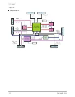
Page 104: ...31Pin LVDS SPS NIRB ASIC 816P DDR FA DDR MA DDR MB MICOM DRIVE RESET R G B 16bit CLK A B BLK POL STB R G B 16bit CLK A B BLK POL STB DATA 32bit ADDR 12bit DQS CLK nCLK RELAY_EINT AC OFF EINT Vs ON LVDS SIGNAL SDA SCL TX RX X MAIN CONTROL SIGNAL Y MAIN CONTROL SIGNAL ADC 4bit ADC 3bit ADC 1bit 4pin I2C 30MHz 60MHz 74MHz 50pin Connector 30pin Connector ...

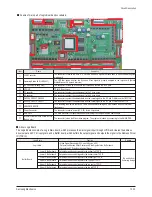
Page 105: ...nector to receive power 5V 3 3V for the Logic board ASIC CHIP The main processor that generates and outputs the logic drive signal and the address data MICOM LOADING 5PIN CONNECTOR Debug only The connector to load the Micom drive program The program is loaded by connecting to the GA WRITER About Logic Board The Logic Board consists of a Logic Main board which processes the main signal input throug...

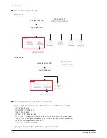
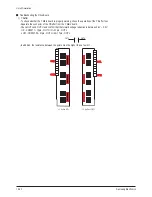
Page 106: ...at the output waveform is normal using an oscilloscope Check if the waveform is the same as shown in Figure 2 by connecting the oscilloscope to the No 12 TP in Figure 1 Check if the waveform is the same as in Figure 3 by connecting the oscilloscope to the connector that is connected to the Buffer board If the measured waveform is different from the following waveforms the board must be replaced To...

Page 107: ...d That is the pixel whose wall charge has been formed by the Address Discharge forms a Sustain Discharge vis the following Sustain pulse 2 Sustain Discharge A Sustain Discharge is a Self Sustaining Discharge formed by the accumulation of the electric potential of the Sustain pulse gen erally 200 210 Volt alternating over the X and Y electrodes during the sustain period and the wall charge dependin...

Page 108: ...d Operation Power Supplied from the power board The optimal value may differ from the following a Vs 205V Sustain b Vset 195V Y Rising Ramp c Ve 100V Ve bias d Vscan 190V Scan low bias e Vnf 175V Y falling Ramp Created by the DC DC power block of the Y Drive board f Vsc_h 70V Scan high bias Created by the DC DC power block of the Y Drive board g Vdd 5V Logic signal buffer IC and IPM h Vcc 15V Gate...

Page 109: ...t and 2 Ve bias in the Scan section is maintained 2 Y Drive Board This is connected to the Y port part of the panel It outputs 1 Sustain voltage wave form including ERC and 2 Y Rising Falling Ramp waveform and maintains 3 Vscan bias 3 Y Buffer Board Upper Lower This board supplies the Scan waveform to the Y port and consists of Upper and Lower boards For an HD grade unit 6 scan driver ICs TEXAS IN...

Page 110: ...FPC output electrodes sequentially one line at a time At this time Vscan is called the Scan Bias Voltage A Vscan voltage of approximately 175 Volt Vsc_1 is supplied to the electrode lines For the other lines 56 volt Vsc_h is higher than Vscan l by 120V is supplied However negative wall charges are accumulated on the Y electrode by the Ramp pulse and positive wall charges are accumulated on the add...

Page 111: ...ance 0 2 When no signal is output to the gate GND FET changes to an open circuit i e an insulator of resistance High Voltage Switching of the FET Operation 1 When no signal is applied to G1 FET1 is opened and when the signal is applied to G2 FET2 short circuits GND is output via the output terminal 2 When a signal is applied to G1 FET1 short cir cuits and when no signal is applied to G2 FET2 is op...

Page 112: ...Circuit Description 13 20 Samsung Electronics Drive Board Connector Layout 1 X Main ...

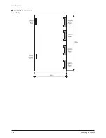
Page 113: ...Circuit Description Samsung Electronics 13 21 2 Y Main CN5007 Power CN5008 Signal CN5010 CN5009 CN5503 Panel CN5502 CN5501 Panel Panel CN5403 Panel CN5402 Panel CN5401 Panel CN5507 265mm 320mm CN5407 ...

Page 114: ... Y Buffer first Separate the connector of the Y Buffer from the Y Main board Check OUTL and OUTH and confirm that the forward voltage reduction is between 0 4V 0 5V UP CN5407 1 10pin OUTH 11 33pin OUTL LOW CN5507 50 41pin OUTH 40 17pin OUTL In addition the resistance between the points must be higher than a few kΩ OUTL OUTH OUTL OUTH OUTL OUTH Y buffer UP Y buffer LOW ...

Page 115: ...cription Samsung Electronics 13 23 2 Y Main Connect the Y Main and Y Buffer and confirm that the output from TP CN5410 CN5411 of the Y Buffer UP is the same as Attachment 1 when the power is supplied CN5410 CN5411 ...

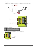
Page 116: ...e in the figure The Vsc_h and Vnf voltages are controlled by the DC DC power part of the Y Main board Voltage Adjustment Specifications 100us 40us Rising Ramp Falling Ramp Y Main Board IPM DC DC Falling Ramp Variable resistor Rising Ramp Variable resistor 100us 40us Y Main Board Vsc_h TP DC DC Vset Vs Vsc_l Vsc_h Ve Va 200V 205V 175V 56V 105V 70V ...

Page 117: ...Circuit Description Samsung Electronics 13 25 3 X Check that the output of X Out of the X board follows the waveform of Attachment 2 when the power is supplied XOUT ...

Page 118: ...Circuit Description 13 26 Samsung Electronics Attachment 1 Y Output Waveform The Scan Waveform Must Be Observed Y Output Waveform 200us div 100V div 1us div 100V div Sustain Waveform ...

Page 119: ...Circuit Description Samsung Electronics 13 27 Attachment 2 X Output Waveform X Output Waveform 200us div 100V div 2us div 100V div Sustain Waveform ...

Page 120: ...2550 and is currently being used in LCD TVs It also uses SMBUS which is the same type as I2C for communication The Ambient Light Sensor can detect up to 1846 Lux in normal mode The data of the sensor can be measured for Lux operations once every 800ms Control is implemented by using R_ASL_GAIN The number of sustain pulses moves left or right as shown in the figure on the right For a low gradation ...

Page 121: ...umber of sustain pulses according to the ASL Average Signal Level by R_P_Lower_Gain value In the PDP Logic R_Multi_APC is set to 0X01 Multi_APC operates and R_P_CM_Gain_SW is set to 0X01 so that the upper and lower limits of the APC Table can be shifted by adjusting the R_P_Lower_Gain value only Therefore the sustain pulse is controllable for the white pattern even though it was formerly not contr...

Page 122: ...13 30 Samsung Electronics MEMO ...

Page 123: ...able is longer than for normal use check the visual quality of the video on the screen and shorten the length if necessary This also applies to the PC RGB D Sub cable When the length of the cable is longer than for normal use video may not be displayed on the screen In this case shorten the cable length When a digitally distributed TV user receives HD rated broadcasts The digital distributed TV Re...

Page 124: ...er or game console through a wide TV by selecting the aspect ratio to normal 4 3 or wide 21 9 the left and right or top and bottom of the picture will not be displayed This symptom appears in other manufacturer s TV s The three appliance companies are trying to resolve the problem through the Ministry of Information and Communication Changing the Order of the Picture Size for 16 9 Display Devices ...

Page 125: ...ng is a television broadcasting signal digitized and transmitted according to the United States terrestrial digital broadcast standard or ATSC Mono A type of audio interface that transmits the audio signal through a single channel only Through a mono interface it is hard to experience stereophonic sound and the sound is played using only one speaker Reception Sensitivity Amplification LNA A signal...

Page 126: ...provide clearer and sharper visual quality Anynet Anynet is an AV network system that enables an easy to use AV interface for users by controlling all connected AV devices through the Anynet menu when the AV devices of Samsung Electronics are connected DVD Digital Versatile Disc DVD is a large capacity storage media that can store multime dia content such as video games audio applications etc usin...

Page 127: ...hree primary colors of light R G and B the number of possible colors for a pixel is 256 x 256 x 256 16 777 216 or 16 7 million colors If 12 bits are used for a pixel the gradation is 212 or 4096 for a color Since three colors R G and B are used 4096 x 4096 x 4096 or 68 7 billion colors are support ed per pixel Since 68 7 billion colors are far more than 16 7 million colors the picture will be disp...

Page 128: ...a of the signal broadcast from a broadcast station is smaller than that of possible color coordinates Moreover a TV provides a smaller color coordinate area than that of the signal from the broadcasting station even though the size of the color coordinate area varies depending on the TV model In general Color Reproductivity is used as follows The Color reproductivity of a TV is a certain of NTSC T...

Reviews: