Circuit Description
13-16
Samsung Electronics
■
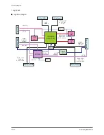
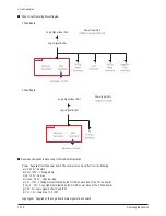
Drive Circuit Operating Block Diagram
- Y Drive Board
Power Input Part
Logic Signal Input Part
Logic Signal Buffer
Power Input Part
Logic Signal Input Part
Logic Signal Buffer
- X Drive Board
■
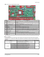
Requisite Components Necessary for Drive Board Operation
- Power : Supplied from the power board. The optimal value may differ from the following:
a) Vs : 205V - Sustain
b) Vset : 195V - Y Rising Ramp
c) Ve : 100V - Ve bias
d) Vscan : -190V - Scan low bias
e) Vnf : -175V - Y falling Ramp (Created by the DC-DC power block of the Y Drive board)
f) Vsc_h : -70V - Scan high bias (Created by the DC-DC power block of the Y Drive board)
g) Vdd : 5V - Logic signal buffer IC and IPM
h) Vcc : 15V - Gate drive IC ¹× IPM
- Logic Signal : Supplied by the Logic board. Gate signal of each switch
Summary of Contents for HP-R5052
Page 14: ...1 6 Samsung Electronics MEMO ...
Page 40: ...3 20 Samsung Electronics MEMO ...
Page 43: ...Samsung Electronics 5 2 MEMO ...
Page 51: ...6 8 Samsung Electronics MEMO ...
Page 59: ...8 4 Samsung Electronics MEMO ...
Page 61: ...9 2 Samsung Electronics MEMO ...
Page 84: ...11 12 Samsung Electronics MEMO ...
Page 92: ...12 8 Samsung Electronics MEMO ...
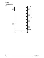
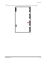
Page 112: ...Circuit Description 13 20 Samsung Electronics Drive Board Connector Layout 1 X Main ...
Page 122: ...13 30 Samsung Electronics MEMO ...


