


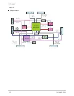


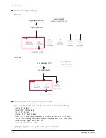


Circuit Description
13-10
Samsung Electronics
Control
and
Switching Block
Control
and
Switching Block
Control
and
Switching Block
Transformer
Transformer
Transformer
Auxiliary
Power
Auxiliary
Power
Auxiliary
Power
Rectification
Block
Rectification
Block
Rectification
Block
Feedback
Block
Feedback
Block
Feedback
Block
Vs Input Part
Vscan Output
Vset Output
Ve Output
(-175~-220)
DC DC SMPS receives Vs input (195~215V) from the Main SMPS and the necessary Vscan, Vset and Ve voltages are output to
operate the PDP Module as shown in the block diagram above.
1. Block Diagram
Summary of Contents for HP-R5052
Page 14: ...1 6 Samsung Electronics MEMO ...
Page 40: ...3 20 Samsung Electronics MEMO ...
Page 43: ...Samsung Electronics 5 2 MEMO ...
Page 51: ...6 8 Samsung Electronics MEMO ...
Page 59: ...8 4 Samsung Electronics MEMO ...
Page 61: ...9 2 Samsung Electronics MEMO ...
Page 84: ...11 12 Samsung Electronics MEMO ...
Page 92: ...12 8 Samsung Electronics MEMO ...
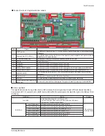
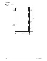
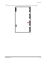
Page 112: ...Circuit Description 13 20 Samsung Electronics Drive Board Connector Layout 1 X Main ...
Page 122: ...13 30 Samsung Electronics MEMO ...


