Circuit Description
Samsung Electronics
13-13
■
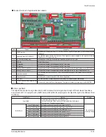
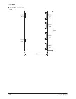
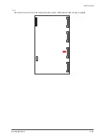
A name of main part of Logic Board and vocabulary.
Item
Name
Description
①
LVDS Connector
The connector to receive the RGB, H, V, DATAEN and DCLK signals that have been LVDS encoded through the
main board.
②
Operating Status LED (LED2001)
The LED that shows whether the Sync and Clock signal is properly supplied to the logic board (Normal
Status:Blinks at 0.8 second intervals)
③
I2C Connector (Debug only)
The connector for the Key Scan board that checks and controls the 512K data.
④
V-TOGG
TP for V Sync Check
⑤
Y Connector
The connector to output the control signal for the Y drive board.
⑥
X Connector
The connector to output the control signal for the X drive board.
⑦
CN2006, CN2007, CN2008
The connector to output the address data and the control signal to the E,F and G-buffer board of BOTTOM.
⑧
CN2009, CN2010, CN2011
The connector to output the address data and the control signal to the E,F and G-buffer board of TOP.
⑨
ARM-PROCESSOR
512K including the Gamma Table, APC Table, drive waveform timing and other options is saved to internal
flashmemory.
⑩
Power Connector
The connector to receive power (5V, 3.3V) for the Logic board.
⑪
ASIC CHIP
The main processor that generates and outputs the logic drive signal and the address data.
⑫
MICOM LOADING 5PIN CONNECTOR
(Debug only)
The connector to load the Micom drive program. The program is loaded by connecting to the GA-WRITER.
■
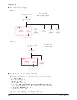
About Logic Board
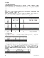
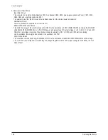
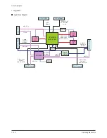
The Logic Board consists of a Logic Main board, which processes the main signal input through LVDS and creates the address
driver output and X,Y drive signals, and a Buffer board, which buffers the output signal and outputs the signal to the Address Driver
IC (TCP IC).
Logic Board
Function
Remark
Logic Main
- Video Signal Processing (W/L, error diffusion, APC)
- Outputs the Address Driver Control and Data Signals to the Buffer board.
- Outputs the XY Drive Board Control Signal
Buffer Board
Lower E Buffer board
Outputs data and control signals to the bottom left TCP IC.
Top and bottom
Symmetry design
Lower F Buffer board
Outputs data and control signals to the bottom center TCP IC.
Lower G Buffer board
Outputs data and control signals to the bottom right TCP IC.
Upper E Buffer board
Outputs data and control signals to the Top right TCP IC.
Upper F Buffer board
Outputs data and control signals to the top center TCP IC.
Upper G Buffer board
Outputs data and control signals to the top left TCP IC.
Summary of Contents for HP-R5052
Page 14: ...1 6 Samsung Electronics MEMO ...
Page 40: ...3 20 Samsung Electronics MEMO ...
Page 43: ...Samsung Electronics 5 2 MEMO ...
Page 51: ...6 8 Samsung Electronics MEMO ...
Page 59: ...8 4 Samsung Electronics MEMO ...
Page 61: ...9 2 Samsung Electronics MEMO ...
Page 84: ...11 12 Samsung Electronics MEMO ...
Page 92: ...12 8 Samsung Electronics MEMO ...
Page 112: ...Circuit Description 13 20 Samsung Electronics Drive Board Connector Layout 1 X Main ...
Page 122: ...13 30 Samsung Electronics MEMO ...


