Circuit Description
13-8
Samsung Electronics
2. Description of Each Block
- Input Filter Circuit
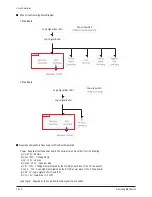
This consists of a Common Mode Reactor LF801, X-condenser C803, C804, Line by-pass condenser(Y con), C801, C802,
C823, C824 and a lightning conductor, Z801.
The external noise from the AC line and the feedback noise from the internal power are reduced.
- Rectification Circuit
Converts (rectifies) the supplied AC current into DC.
- MAIN SWITCHING Circuit Block
Transmits the energy of the electrolytic capacitor (C805) to the secondary coil, T801 [MAIN TRANS], by turning the MOS-FET
embedded in U802 (5M0565R) on or off for PWM power, and generates a DC output voltage of +5.3V, +6.5V, +12V and +30V.
When the input voltage is supplied, the activation voltage is supplied to Pin 3 of U802, and U802 starts oscillating.
Via the oscillation, the energy is transmitted to the secondary coil, T801.
- DC-DC Circuit Block
The circuit that converts the energy transmitted to T801 via the oscillation of the MAIN SWITCHING U802 into DC voltage.
The +6.5V and +12V voltages are controlled by the Voltage Regulator and the +30V output voltage is controlled by the Turn
Ratio of T801.
Summary of Contents for HP-R5052
Page 14: ...1 6 Samsung Electronics MEMO ...
Page 40: ...3 20 Samsung Electronics MEMO ...
Page 43: ...Samsung Electronics 5 2 MEMO ...
Page 51: ...6 8 Samsung Electronics MEMO ...
Page 59: ...8 4 Samsung Electronics MEMO ...
Page 61: ...9 2 Samsung Electronics MEMO ...
Page 84: ...11 12 Samsung Electronics MEMO ...
Page 92: ...12 8 Samsung Electronics MEMO ...
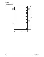
Page 112: ...Circuit Description 13 20 Samsung Electronics Drive Board Connector Layout 1 X Main ...
Page 122: ...13 30 Samsung Electronics MEMO ...


