Circuit Description
Samsung Electronics
13-17
■
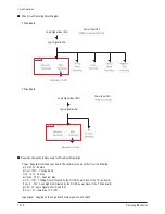
Drive Circuit Architecture and Function Description
- Description of the function of each board
1) X Drive Board
This is connected to the X port part of the panel. 1) Sustain voltage waveform (including ERC) is output, and 2) Ve bias in the Scan
section is maintained.
2) Y Drive Board
This is connected to the Y port part of the panel. It outputs 1) Sustain voltage wave form (including ERC), and 2) Y Rising, Falling
Ramp waveform, and maintains 3) Vscan bias.
3) Y Buffer Board (Upper, Lower)
This board supplies the Scan waveform to the Y port and consists of Upper and Lower boards. For an HD grade unit, 6 scan
driver ICs (TEXAS INSTRUMENT SN755867APZP: 64 outputs) are mounted on the board.
Summary of Contents for HP-R5052
Page 14: ...1 6 Samsung Electronics MEMO ...
Page 40: ...3 20 Samsung Electronics MEMO ...
Page 43: ...Samsung Electronics 5 2 MEMO ...
Page 51: ...6 8 Samsung Electronics MEMO ...
Page 59: ...8 4 Samsung Electronics MEMO ...
Page 61: ...9 2 Samsung Electronics MEMO ...
Page 84: ...11 12 Samsung Electronics MEMO ...
Page 92: ...12 8 Samsung Electronics MEMO ...
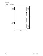
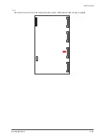
Page 112: ...Circuit Description 13 20 Samsung Electronics Drive Board Connector Layout 1 X Main ...
Page 122: ...13 30 Samsung Electronics MEMO ...


