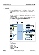


NXP Semiconductors
IMXRT500HDG
i.MX RT500 Hardware Design Guide
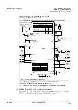
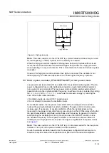
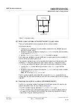
3.3 i.MX RT500 power domains, internal regulator
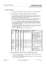
The
LDO_ENABLE
input signal is listed in this power domain section because it is the
control signal that enables the internal
VDDCORE LDO
regulator when an external
VDDCORE
supply is not used. This pin is pulled high to enable the internal
LDO
and tied
low when an external supply provides
VDDCORE
.
Along with the minimum quantities of bulk and decoupling capacitors, we must see
on where to place the capacitors and parametric recommendations for the capacitors.
In the high-speed designs, which use ball-grid array packaging, the balls are soldered to
the top layer, the signals are routed on at least two layers, and the power pins are routed
on two or more other layers. The area directly below the MCU on the bottom layer is
where most, if not all, of the decoupling capacitors should be connected to the ground
and power domains.
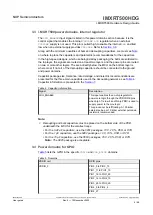
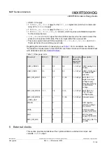
Capacitor package size, tolerance, rated voltage, and dielectric recommendations are
presented for the three main capacitors used in the decoupling networks, see
.
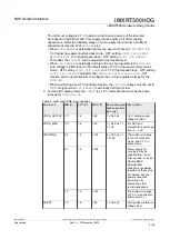
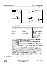
Capacitor information is presented in the
Signal
Description
LDO_ENABLE
This input enables the on-chip regulator to
power core logic through the VDDCORE pins
when high. Tie low if an off-chip PMIC is used to
supply power to the core logic.
This pin cannot be left floating. A 100 kohm
external pull-up or 10 kohm external pull-down
resistor is recommended.
Table 4. Capacitor information
Note:
1. Decoupling and bulk capacitors must be placed on the bottom side of the PCB,
underneath the MCU for the smallest loops.
•
For the 0.22 μF capacitors, use the 0201 packages, 10 V, 20 %, X5R, or X7R
•
For the 1 µF capacitors, use the 0402 packages, 10 V, 10 %, X5R, or X7R
•
For the 10 µF capacitors, use the 0603 packages, 16 V, 20 %, X5R, or X7R
Note:
The 0805 package is acceptable.
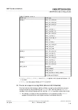
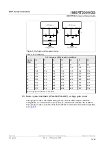
3.4 Power domains for GPIO
lists the GPIO in the specific
VDDIO
and
VDD_AO1V8
domains.
VDDIO rail
GPIO pins
PIO0_0 to PIO0_13
PIO1_11 to PIO1_15
PIO1_18 to PIO1_29
PIO2_14 to PIO2_15
PIO3_25 to PIO3_29
PIO4_0 to PIO4_6
VDDIO_0
PIO6_27
Table 5. Domains
IMXRT500HDG
All information provided in this document is subject to legal disclaimers.
© 2022 NXP B.V. All rights reserved.
User guide
Rev. 0 — 15 November 2022
6 / 48


