


NXP Semiconductors
IMXRT500HDG
i.MX RT500 Hardware Design Guide
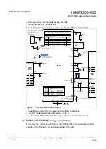
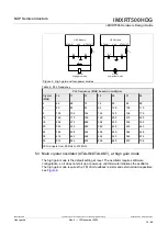
Note:
Higher frequency clocks may show wave deformation due to loading and drive
strength. Full drive strength can be enabled to resolve it.
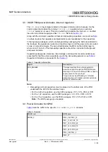
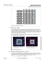
CLKOUT Port
osc_clk
1m_lposc
000
001
FRO_DIV2
010
main_clk
011
dsp_main_clk
100
CLKOUTSEL0
main pll_clk
000
001
aux0 pll_clk
010
dsp pll_clk
011
aux1 pll_clk
100
audio_pll_clk
101
32k_clk
110
CLKOUTSEL1
CLKOUTDIV
CLKOUT
CLKOUT
divider
PIO0_24
PIO1_10
PIO1_19
PIO4_0
PIO2_29
Figure 10. CLKOUT port
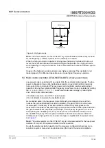
5.9 Oscillator load capacitance
Choosing load capacitor values for a crystal oscillator is a topic that can take more time
to discuss and also to understand. First, let us look at what load capacitance is.
The load capacitance (also called C
L
) of a crystal is different from the load capacitor
values placed on the crystal pins (also called C
x
and C
y
). The crystal load capacitance is
a crystal parameter used by the vendor to manufacture and test each crystal.
Crystal vendors generally specify a range of C
L
values in their data sheets as
manufacturing and test conditions. For example, 32.768 kHz crystal data sheet C
L
values
can range from 9 pF to 12.5 pF. A customer can choose the desired value. It is the
responsibility of the customer to tune the crystal in their circuit. You must know the crystal
C
L
value in order to begin tuning.
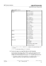
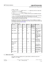
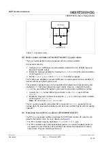
Load capacitors C
x
and C
y
are placed from the crystal legs to the ground. While it may
look like these caps are in parallel, they are actually in series across the crystal, see
.
aaa-046628
XOUT
XIN
XTAL
Cy
Cx
RTxxx
Oscillator
Figure 11. Load capacitance
IMXRT500HDG
All information provided in this document is subject to legal disclaimers.
© 2022 NXP B.V. All rights reserved.
User guide
Rev. 0 — 15 November 2022
18 / 48


