


NXP Semiconductors
IMXRT500HDG
i.MX RT500 Hardware Design Guide
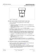
•
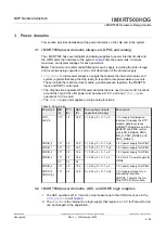
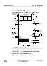
USB 3.3 V supply
•
1.1 V
MIPI_DSI_VDD11
supply for the
MIPI_DSI
digital core (which we recommend
tying to the
VDDCORE
supply)
•
1.8 V
MIPI_DSI_VDD18
supply for the
MIPI_DSI PHY
•
1.8 V
MIPI_DSI_VDD18_VDDA_CAP
domain, which requires a stabilization capacitor
for this internal domain
•
USB1_VBUS
is a 3 V to 5 V signal from the USB connector, which is used to detect the
presence of an active USB cable. This is an input rather than a power rail.
•
There are several internal VSS connections
VSS
,
VSSA
,
MIPI_DSI_VSS
, and
VREFN
that must be tied to a common ground node.
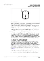
Regarding the termination of unused pins, see
. For more details, see Section
"Termination of unused pins" of
i.MX RT500 Low-Power Crossover Processor Data Sheet
with Addendum
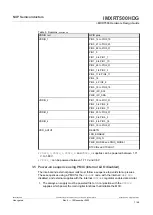
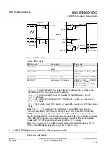
Power rail
MIN (V)
TYP (V)
MAX (V)
Decoupling
and bulk
capacitors
(min qty)
Description
USB1_VDD3V3
3.0
3.3
3.6
1 × 0.22 μF USB1 analog 3.3 V
supply
USB1_VBUS
3.0
5.0
5.5
1 × 0.22 μF USB1_VBUS input
to validate USB
presence
MIPI_DSI_VDD11
0.85
1.1
1.155
1 × 0.22 μF MIPI DSI 1.1 V
digital core input
voltage supply.
Recommend trying
to VDDCORE
voltage.
MIPI_DSI_VDD18 1.71
1.8
1.89
1 × 0.22 μF MIPI DSI 1.8 V
PHY I/O input
voltage supply
MIPI_DSI_VDD18
_VDDA_CAP
—
—
1.155
1 × 0.22 μF Internal domain
VREFN
—
0
—
—
ADC negative
reference voltage.
Tie to GND
VSSA
—
0
—
—
Analog negative
supply. Tie to GND
VSS
—
0
—
—
MCU negative
supply. Tie to GND
MIPI_DSI_VSS
—
0
—
—
MIPI_DSI_VSS. Tie
to GND
Table 7. Other power rails
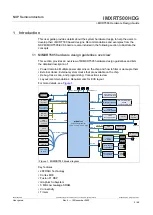
5 External clocks
This section provides details about the crystal oscillators, external clock input, and
versatile
CLKOUT
output.
IMXRT500HDG
All information provided in this document is subject to legal disclaimers.
© 2022 NXP B.V. All rights reserved.
User guide
Rev. 0 — 15 November 2022
12 / 48


