


NXP Semiconductors
IMXRT500HDG
i.MX RT500 Hardware Design Guide
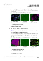
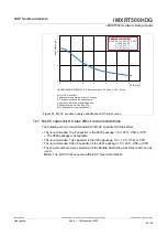
The 12
VDDCORE
balls routed to 4 microvias are highlighted on the left figure. Microvias
are used to connect layers 1-2, 2-3, 3-4, 4-5, and 5-6.
Skip vias are used to connect layers 1-3 and layers 4-6, as shown in the right figure.
Core vias between layers 3 and 4, as shown in
, are larger due to thicker L3 /
L4 dielectric.
Via-in-pad
L 1 to L3
VDDCORE has 12
power balls to 4
microvias
2 common power
balls per microvia
Skip via, L 1 to L3
L3 to L4 microvias
are larger ( called
Core vias) due to
thicker L3/L4
dielectric
Figure 20. HDI recommendations
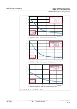
7.11 HDI recommendations, layers - 6
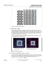
The capacitor quantities directly under the package (bottom layer L6) should generally be
1-per-via decoupling capacitors, plus one or two additional bulk capacitors. It reduces the
number of capacitors from 1-per-pin to 1-per-2 or more pins on some supply domains.
However, when multiple balls share a via, larger decoupling capacitor values should be
used. In this design, we use 0.22 µF ceramic bypass capacitors instead of the 0.1 µF
capacitors normally used on conventional 1 capacitor-per-pin design.
Bulk and decoupling capacitors
located directly underneath the
MCU on the bottom layer.
Figure 21. The bottom layer L6 of the PCB
7.12 HDI implementation
HDI implementation means that there may be a different number of vias from the top
layer to the bottom layer.
Observe the progression from the top to the bottom layers, see
:
IMXRT500HDG
All information provided in this document is subject to legal disclaimers.
© 2022 NXP B.V. All rights reserved.
User guide
Rev. 0 — 15 November 2022
32 / 48


