

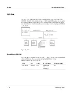


I/O-Bus
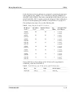
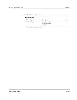
Memory Map and Devices
5 - 20
PPC/PMC-8260/DS1
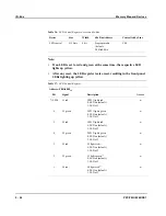
8. Program access to respective mailbox register
PowerQUICC II is then set into the reset state (Powerup_RESET). On-board
glue-logic parks the 60x-bus to the PowerSPAN II and asserts Address
Acknowledge (AACK) together with Partial Data Valid (PSDVAL) and Trans-
fer Acknowledge (TA) to terminate the PowerSPAN II’s access cycles to the
boot flash. No address pipelining is supported by hardware during this time.
9. Program fixed time delay (min. 1 msec) to expire until PowerSPAN II is
allowed to program flash
This time delay is necessary to allow the PowerQUICC II to tristate all signals
and buses, so that the PowerSPAN II can act as the only 60x bus master.
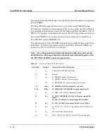
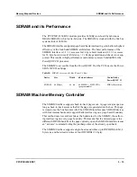
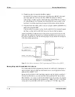
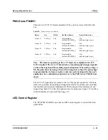
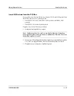
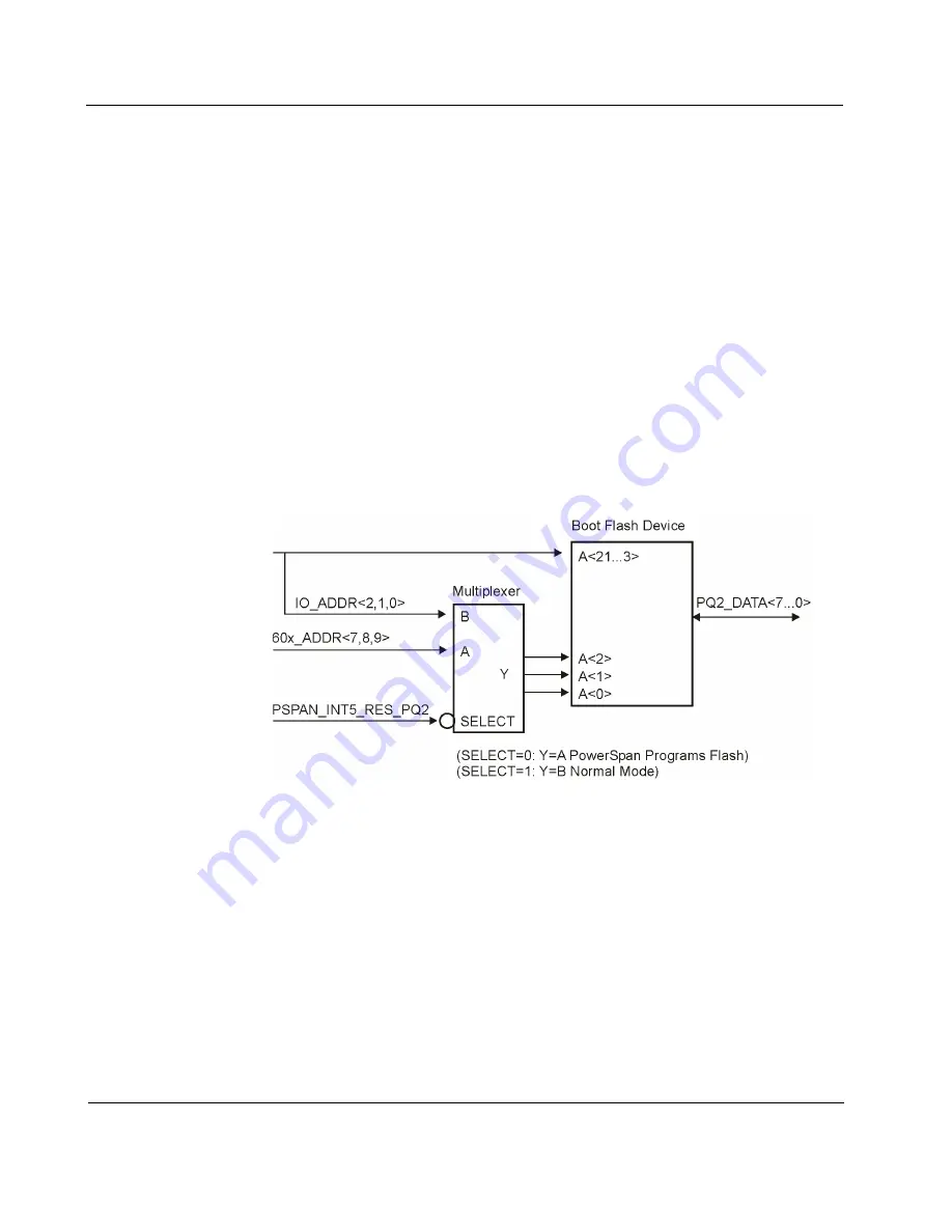
As the PowerSPAN II supports only 64-bit port size devices on the 60x bus side,
high order 60x-addresses connected to an external multiplexer are used to access
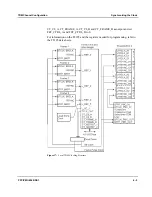
the 8-bit boot flash device. See the following figure for a symbolic block diagram
of the byte address generation.
Figure 16:
Byte Address Generation for Flash Programming from PCI Bus via PowerSPAN II
Memory Map when PowerQUICC II is in Reset
To accommodate the flash programming from the PowerSPAN II a multiplexer is
used to generate the byte addresses for the flash device out of high order 60x bus
addresses 60x_ADDR<7,8,9>.
Because the PowerSPAN II PCI bus bridge supports only 64-bit slaves and the 8-
bit wide boot flash device is connected to the most significant 60x bus byte lane
PQ2_DATA[0...7], accesses to the 8-bit boot flash device must always be targeted
to the 60x-bus least significant byte addresses 60x_ADDR<29,30,31>=000 (which
correspond to byte lane PQ2_DATA[0...7], see Figure 15 “I/O Bus” page 5-18).
Summary of Contents for PPC/PMC-8260/DS1
Page 1: ...PPC PMC 8260 DS1 Reference Guide P N 6806800B10A July 2006 ...
Page 8: ...viii PPC PMC 8260 DS1 ...
Page 22: ...xxii PPC PMC 8260 DS1 ...
Page 26: ...xxvi PPC PMC 8260 DS1 ...
Page 30: ...xxx PPC PMC 8260 DS1 ...
Page 31: ...1 Introduction ...
Page 32: ......
Page 39: ...2 Installation ...
Page 40: ......
Page 53: ...3 Indicators and Connectors ...
Page 54: ......
Page 64: ...On Board Connectors Indicators and Connectors 3 12 PPC PMC 8260 DS1 ...
Page 65: ...4 Firmware ...
Page 66: ......
Page 104: ...Code Examples Firmware 4 40 PPC PMC 8260 DS1 ...
Page 105: ...5 Memory Map and Devices ...
Page 106: ......
Page 132: ...Resetting the Devices Memory Map and Devices 5 28 PPC PMC 8260 DS1 ...
Page 133: ...6 TDM Channel Configuration ...
Page 134: ......
Page 145: ...A Troubleshooting ...
Page 146: ......
Page 148: ...A 4 PPC PMC 8260 DS1 ...
Page 150: ...I 2 PPC PMC 8260 DS1 ...