GV-395 Virtex-II DSP Hardware Accelerator Manual
GV & Associates, Inc.
07/10/04
33
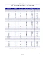
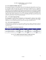
Output Configuration
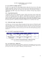
JP4
Offset Binary
Jumper on pin 1 and pin 2
Twos-Complement
Jumper on pin 2 and pin 3
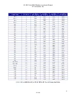
13.1.3.1
GVA-AD9430 Digital Output Format Jumper Configuration Table
13.2
GVA-AD9432 100 MSPS 12 Bit A/D
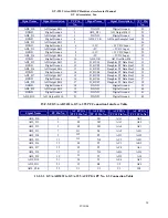
The analog input is injected via a 50-ohm SMA connector (P1). The analog input voltage should not exceed 2 Vp-p.
The input Analog – Digital Converter (AD9432) is protected against accidental application of an over-voltage input
by a protection diodes. The digital data generated by the Analog to Digital Converters is buffered by
74ALVCH16374 (a 16 bit D register). This buffer incurs a one-clock delay between the A/D and the FPGA. This
was necessary to insure proper data setup time for the FPGA. The analog signals are each sampled by a 100 MSPS
analog to digital converter (AD9432). The input sample clock (AD0_CLK) can be set to a maximum frequency of
100 MHz via the Analog Control FPGA (U14). The sample clock may be generated either the 100 MHz system
clock or from the External Clock Input (P6). The LVTTL clock signal is coupled with a differential receiver
(MC10EL16). The output of this differential receiver drive the ENCODE and ENCODE- inputs of the converter and
provides the sub-nanosecond rise times for optimum performance.
13.2.1
AC Coupled Analog Input Path
The analog input is AC coupled into two Mini-Circuits T1:1 transformer, which has a high pass corner at 50 KHz.
These transformers are used to generate a differential input to the AD9432. To reduce the second harmonic
distortion two T1-1T transformers are connected in series. A 3 dB to 4 dB improvement can be realized.
Additionally, an external anti-aliasing filter may be needed to limit the input bandwidth of the A/D.
13.2.2
DC Coupled Analog Input Path
A differential output op amp (AD8138) is used to drive the AD9432 in the dc-coupled configuration. The AD8138
was specifically designed for ADC driver applications and has superior SNR performance in analog frequencies
from 0 thru 30 MHz.
13.2.3
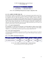
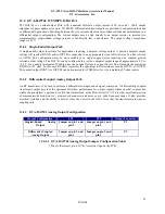
GVA-AD9432 Analog Input Configuration
Input Configuration
JP1
JP2
JP3
AC-Coupled Analog Input
Jumper on pin 1 and
pin 2
Jumper on pin 1 and
pin 2
Jumper on pin 1 and
pin 2
DC-Coupled Analog Input
Jumper on pin 2 and
pin 3
Jumper on pin 2 and
pin 3
Jumper on pin 2 and
pin 3
13.2.3.1
GVA-AD9432 Analog Input Jumper Configuration Table
* Pin 1 is the closest pin to GV & Associates logo on the PCB.

