


ATM AAL1 Circuit Emulation Service
MPC8260 PowerQUICC II Family Reference Manual, Rev. 2
Freescale Semiconductor
31-13
Table 31-1
describes CAS routing table entry fields.
31.4.7.2
TDM-to-ATM CAS Support
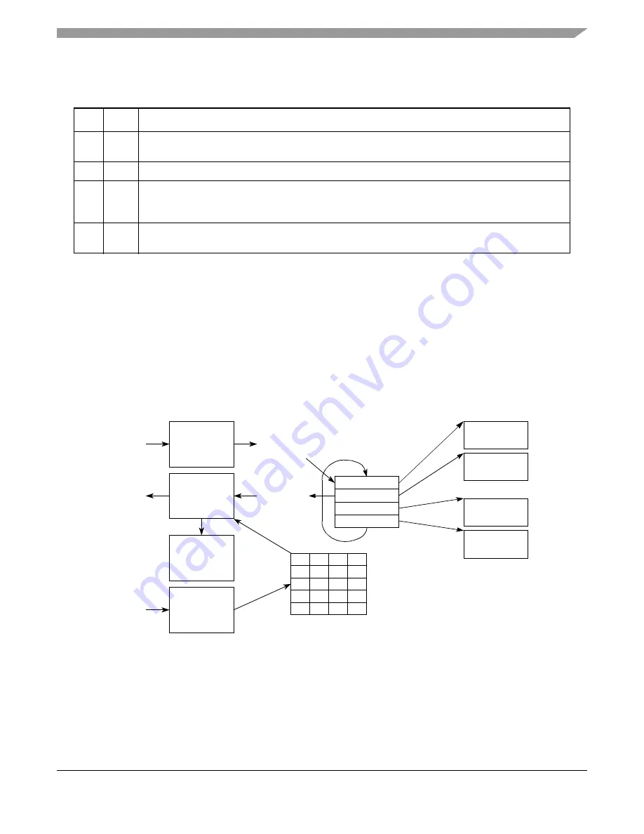
During the segmentation process, the AAL1 CES transmitter reads the CAS data from the internal CAS
block and packs the data and the signaling information at the end of an AAL1 super frame (depicted in
Figure 31-3
). All AAL1 functions operate normally (generating AAL1 PDU-headers, structured pointers,
etc.). Each common (MCC, ATM) BD table should point to buffers that can contain a whole number of
super frames. The last buffer of the super frame is marked as the end of a super frame (BD[EOSF]=1).
After closing a buffer with the EOSF indication, the ATM transmitter processes the CAS data—reads it
from the internal CAS block and inserts it into the cell payload at the transmit side. The EOSF indication
in the BD is statically set by the CPU when initializing the BD table.
Figure 31-12. CAS Flow TDM-to-ATM
The CAS block is automatically written to internal RAM by the MCC receiver using a separate TDM.
When a super frame is received the MCC should be triggered with a super-frame (multi-frame) SYNC
from the external framer. The incoming CAS block should be captured by the MCC only once for each
super frame (on the last frame).
Table 31-1. CAS Routing Table Entry Field Descriptions
Bits
Name
Description
0
W
Wrap bit. When set, this bit indicates the last circular table entry. During initialization, the host must clear
all W bits in the table except the last one, which must be set.
1
—
Reserved, should be cleared during initialization.
2
F/S
First/Second.
0 Indicates that the signaling information occupies the
first nibble
in the CAS block (LSB).
1 Indicates that the signaling information occupies the
second nibble
in the CAS block (MSB).
3-7
SOP
Signaling Offset Pointer. Offset of the signaling nibble from the internal CAS base address.
Note that in ESF mode the maximum offset is 23 and in E1 framing format the maximum offset is 31.
EOSF
EOSF
Buffer 1
Buffer 2
Buffer 3
Buffer 4
MCC
Rx
Data I/F
T1/E1 framer
MCC
Rx pointer
ATM
Tx pointer
ATM
Tx
UTOPIA
interface
BD table per VC
MCC
Rx
Incoming CAS block per trunk
(internal RAM)
Transmit
CAS routing
table
Super
frame
Super
frame
CAS serial I/F
T1/E1 framer
Shown in
Figure 1-10
Note: With CAS only 4 T1/E1 are supported.
Summary of Contents for MPC8250
Page 90: ...MPC8260 PowerQUICC II Family Reference Manual Rev 2 lxxxviii Freescale Semiconductor...
Page 94: ...MPC8260 PowerQUICC II Family Reference Manual Rev 2 I 4 Freescale Semiconductor...
Page 118: ...Overview MPC8260 PowerQUICC II Family Reference Manual Rev 2 1 24 Freescale Semiconductor...
Page 236: ...Reset MPC8260 PowerQUICC II Family Reference Manual Rev 2 5 14 Freescale Semiconductor...
Page 274: ...60x Signals MPC8260 PowerQUICC II Family Reference Manual Rev 2 7 18 Freescale Semiconductor...
Page 548: ...MPC8260 PowerQUICC II Family Reference Manual Rev 2 IV 8 Freescale Semiconductor...
Page 1072: ...ATM AAL2 MPC8260 PowerQUICC II Family Reference Manual Rev 2 32 10 Freescale Semiconductor...
Page 1356: ...MPC8260 PowerQUICC II Family Reference Manual Rev 2 Index 28 Freescale Semiconductor U U Index...


