


Chapter 2 Port Integration Module (S12XEP100PIMV1)
MC9S12XE-Family Reference Manual , Rev. 1.19
152
Freescale Semiconductor
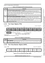
NOTE
Due to internal synchronization circuits, it can take up to 2 bus clock cycles
until the correct value is read on PTH or PTIH registers, when changing the
DDRH register.
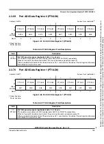
2.3.64
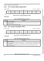
Port J Reduced Drive Register (RDRJ)
1
DDRJ
Port J data direction
—
This register controls the data direction of pin 1.
The enabled SCI2 forces the I/O state to be an output. The DDRM bits revert to controlling the I/O direction of a pin
when the associated peripheral module is disabled.
1 Associated pin is configured as output.
0 Associated pin is configured as input.
0
DDRJ
Port J data direction
—
This register controls the data direction of pin 0.
The enabled SCI3 or CS3 signal forces the I/O state to be an output. In those cases the data direction bits will not
change. The DDRM bits revert to controlling the I/O direction of a pin when the associated peripheral module is
disabled.
1 Associated pin is configured as output.
0 Associated pin is configured as input.
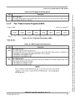
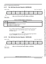
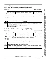
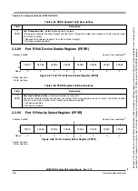
Address 0x026B
Access: User read/write
(1)
1. Read: Anytime.
Write: Anytime.
7
6
5
4
3
2
1
0
R
RDRJ7
RDRJ6
RDRJ5
RDRJ4
RDRJ3
RDRJ2
RDRJ1
RDRJ0
W
Reset
0
0
0
0
0
0
0
0
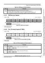
Figure 2-62. Port J Reduced Drive Register (RDRJ)
Table 2-60. RDRJ Register Field Descriptions
Field
Description
7-0
RDRJ
Port J reduced drive
—Select reduced drive for outputs
This register configures the drive strength of output pins 7 through 0 as either full or reduced. If a pin is used as input
this bit has no effect.
1 Reduced drive selected (approx. 1/5 of the full drive strength).
0 Full drive strength enabled.
Table 2-59. DDRJ Register Field Descriptions (continued)
Field
Description
Because
of
an
order
from
the
United
States
International
Trade
Commission,
BGA-packaged
product
lines
and
part
numbers
indicated
here
currently
are
not
available
from
Freescale
for
import
or
sale
in
the
United
States
prior
to
September
2010:
S12XE
products
in
208
MAPBGA
packages


