

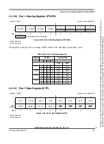


Chapter 2 Port Integration Module (S12XEP100PIMV1)
MC9S12XE-Family Reference Manual , Rev. 1.19
Freescale Semiconductor
165
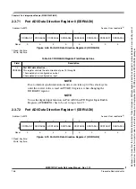
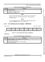
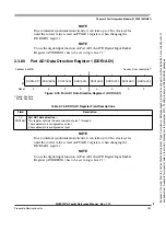
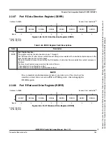
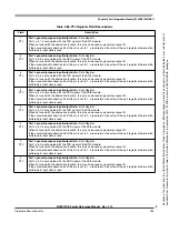
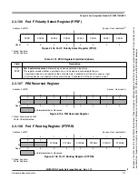
2.3.87
Port R Data Direction Register (DDRR)
NOTE
Due to internal synchronization circuits, it can take up to 2 bus clock cycles
until the correct value is read on PTR or PTIR registers, when changing the
DDRR register.
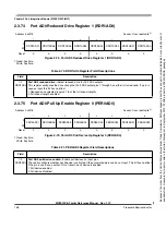
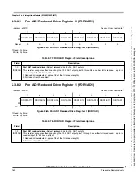
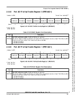
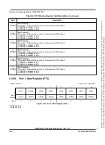
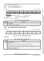
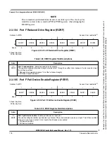
2.3.88
Port R Reduced Drive Register (RDRR)
Address 0x036A
Access: User read/write
(1)
1. Read: Anytime.
Write: Anytime.
7
6
5
4
3
2
1
0
R
DDRR7
DDRR6
DDRR5
DDRR4
DDRR3
DDRR2
DDRR1
DDRR0
W
Reset
0
0
0
0
0
0
0
0
Figure 2-85. Port R Data Direction Register (DDRR)
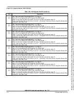
Table 2-83. DDRR Register Field Descriptions
Field
Description
7-0
DDRR
Port R data direction
—
This register controls the data direction of pins 7 through 0.
The TIM forces the I/O state to be an output for each timer port associated with an enabled output compare. In this
case the data direction bits will not change.
The data direction bits revert to controlling the I/O direction of a pin when the associated timer output compare is
disabled.
The timer Input Capture always monitors the state of the pin.
1 Associated pin is configured as output.
0 Associated pin is configured as high-impedance input.
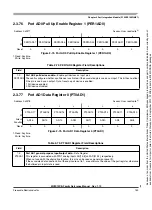
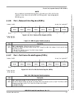
Address 0x036B
Access: User read/write
(1)
1. Read: Anytime.
Write: Anytime.
7
6
5
4
3
2
1
0
R
RDRR7
RDRR6
RDRR5
RDRR4
RDRR3
RDRR2
RDRR1
RDRR0
W
Reset
0
0
0
0
0
0
0
0
Figure 2-86. Port R Reduced Drive Register (RDRR)
Because
of
an
order
from
the
United
States
International
Trade
Commission,
BGA-packaged
product
lines
and
part
numbers
indicated
here
currently
are
not
available
from
Freescale
for
import
or
sale
in
the
United
States
prior
to
September
2010:
S12XE
products
in
208
MAPBGA
packages


