


Appendix A Electrical Characteristics
MC9S12XE-Family Reference Manual , Rev. 1.19
1244
Freescale Semiconductor
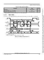
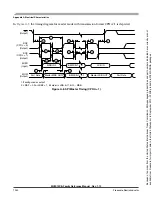
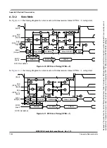
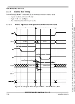
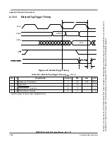
A.7.2.2
Slave Mode
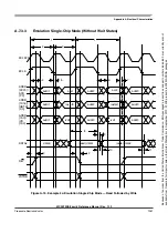
In
the timing diagram for slave mode with transmission format CPHA = 0 is depicted.
Figure A-10. SPI Slave Timing (CPHA = 0)
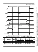
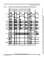
In
the timing diagram for slave mode with transmission format CPHA = 1 is depicted.
Figure A-11. SPI Slave Timing (CPHA = 1)
SCK
(Input)
SCK
(Input)
MOSI
(Input)
MISO
(Output)
SS
(Input)
1
9
5
6
MSB IN
Bit MSB-1 . . . 1
LSB IN
Slave MSB
Slave LSB OUT
Bit MSB-1. . . 1
11
4
4
2
7
(CPOL = 0)
(CPOL = 1)
3
13
NOTE: Not defined
12
12
11
See
13
Note
8
10
See
Note
SCK
(Input)
SCK
(Input)
MOSI
(Input)
MISO
(Output)
1
5
6
MSB IN
Bit MSB-1 . . . 1
LSB IN
MSB OUT
Slave LSB OUT
Bit MSB-1 . . . 1
4
4
9
12
13
11
(CPOL = 0)
(CPOL = 1)
SS
(Input)
2
12
13
3
NOTE: Not defined
Slave
7
8
See
Note
Because
of
an
order
from
the
United
States
International
Trade
Commission,
BGA-packaged
product
lines
and
part
numbers
indicated
here
currently
are
not
available
from
Freescale
for
import
or
sale
in
the
United
States
prior
to
September
2010:
S12XE
products
in
208
MAPBGA
packages