background image

Source Format:

Operation:

OP-Code:

Type:

Clock Cycles:

Flag:

Description:

Example:

Source Format:

Operation:

OP-Code:

Type:

Clock Cycles:

Flag:

Description:

Example:

MSB

LSB

MSB

LSB

40

EPSON

S1C6200/6200A CORE CPU MANUAL

3  INSTRUCTION SET

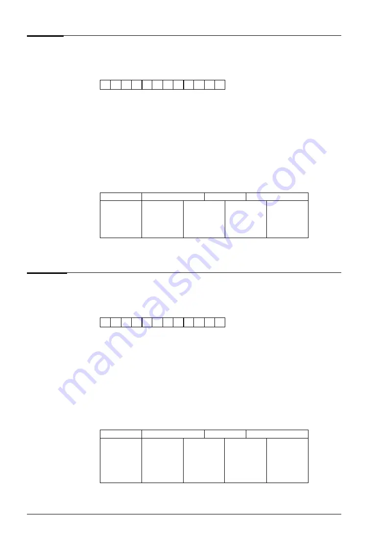
FAN  r,i

Logical AND immediate data i with r-register for flag check

FAN  r,i

 i

3

 to i

0

1

1

0

1

1

0

r

1

r

0

i

3

i

2

i

1

i

0

D80H to DBFH

II

7

Not affected
Set if the result is zero; otherwise, reset.
Not affected
Not affected

Performs a logical AND operation between immediate data i and the contents of
the r-register. Only the Z flag is affected. The r-register remains unchanged.

FAN  A,7

FAN  MY,9

FAN  B,2

A register

1000

1000

1000

1000

B register

0100

0100

0100

0100

Memory (MY)

1000

1000

1000

1000

C flag

1

1

1

1

Z flag

0

1

0

1

FAN  r,q

Logical AND q-register with r-register for flag check

FAN  r,q

 q

1

1

1

1

0

0

0

1 r

1

r

0

q

1

q

0

F10H to F1FH

IV

7

Not affected
Set if the result is zero; otherwise, reset.
Not affected
Not affected

Performs a logical AND operation between the contents of the q-register and the
contents of the r-register. Only the Z flag is affected. The registers remains
unchanged.

FAN  A,B

FAN  MX,B

FAN  A,MY

A register

1000

1000

1000

1000

B register

1010

1010

1010

1010

Memory (MX)

0101

0101

0101

0101

Memory (MY)

1110

1110

1110

1110

C flag

0

0

0

0

Z flag

0

0

1

0

Summary of Contents for S1C6200

Page 1: ...MF297 07 Core CPU Manual CMOS 4 BIT SINGLE CHIP MICROCOMPUTER S1C6200 6200A ...

Page 2: ...uiring high level reliability such as medical products Moreover no license to any intellectual property rights is granted by implication or otherwise and there is no representation or warranty that anything made in accordance with this material will be free from any patent or copyright infringement of a third party This material or portions thereof may contain technology or the subject relating to...

Page 3: ...1C6N3B0 S1C62440 S1C624A0 S1C6S460 Previous No E0C6247 E0C6248 E0C6S48 E0C624C E0C6251 E0C6256 E0C6292 E0C6262 E0C6266 E0C6274 E0C6281 E0C6282 E0C62M2 E0C62T3 New No S1C62470 S1C62480 S1C6S480 S1C624C0 S1C62N51 S1C62560 S1C62920 S1C62N62 S1C62660 S1C62740 S1C62N81 S1C62N82 S1C62M20 S1C62T30 Comparison table between new and previous number of development tools Development tools for the S1C60 62 Fam...

Page 4: ......

Page 5: ... 2 Data Memory 8 2 2 1 Data memory addressing 8 2 3 ALU Arithmetic Logic Unit and Registers 10 2 3 1 D decimal flag and decimal operations 10 2 3 2 A and B registers 11 2 4 Timing Generator 11 2 4 1 HALT and SLP sleep modes 11 2 5 Interrupts 12 2 5 1 Interrupt vectors 12 2 5 2 I interrupt flag 12 2 5 3 Operation during interrupt generation 12 2 5 4 Initial reset 15 3 INSTRUCTION SET ______________...

Page 6: ......

Page 7: ...program memory ROM UP to 4 096 4 bit words of data memory RAM peripheral circuits Memory mapped I O 5 7 or 12 clock cycle instructions 109 instructions Up to 85 levels of subroutine nesting 8 bit stack pointer Up to 15 interrupt vectors Two standby modes Low power CMOS process 1 2 Instruction Set Features Four addressing modes one direct two indirect and one stack pointer Direct addressing transfe...

Page 8: ...bit address bus 4 bit data bus 12 bit data bus Stack Pointer 8 XHL 8 YHL 8 RP 4 Program Counter Block Micro Instructions Instruction Decorder Instruction Register 12 Program Memory ROM 8 192 12 bit words max Data Memory RAM Peripheral I O 4 096 4 bit words max A 4 TEMPB 5 B 4 TEMPA 5 Interrupt Controller Timing Generator Oscillator XP 4 YP 4 ...

Page 9: ...Step 1 to 15 Bank 0 Page 0 Step 0 to 255 Bank 1 Page 1 Step 1 to 15 Bank 1 Page 0 Step 0 to 255 Address Function Reset vector Interrupt vectors used while a program is running in bank 0 Bank 0 page 0 area Direct call subroutines for use by CALZ while a program is running in bank 0 Interrupt vectors used while a program is running in bank 1 Bank 1 page 0 area Direct call subroutines for use by CALZ...

Page 10: ... 1 1 Program counter configuration PCB PCP and PCS together from a 13 bit counter which can address any location in program memory PCP and PCS together from a 12 bit counter which can address any location within a given bank of pro gram memory Each time an instruction other than a jump is executed this counter increments by one Thus a jump instruction does not need to be executed between the last ...

Page 11: ...PSET loads the four low order bits page part of its 5 bit operand to NPP new page pointer and loads the high order bit bank part to NBP new bank pointer Executing a JP instruction immediately after PSET causes a jump to the bank specified by NBP the page specified by NPP and the step specified by the JP instruction operand See Figure 2 1 4 1 Page 15 Bank 0 Page 14 PSET JUMP Bank 0 Step 0 Step 1 St...

Page 12: ... 0 The data set by PSET is canceled and the program jumps to bank 0 page 1 step 9 Bank Page Stap Instruction PSET JP PSET NOP5 JP SCF PSET JP RFC PSET JP JP 13H 08H 15H 09H 14H C 07H 05H C 08H 09H 0 0 0 0 0 0 0 0 0 0 0 0 01H 01H 01H 01H 01H 01H 01H 01H 01H 01H 01H 01H 10H 11H 21H 22H 23H 55H 56H 57H 60H 61H 62H 63H 2 1 7 CALZ instruction CALZ is a direct subroutine call instruction It calls a subr...

Page 13: ...8 RET and RETS instructions The RET instruction causes a return from a subroutine to the address immediately following the address from where that subroutine was called The RETS instruction causes a return to the address following this address Proper use of RET and RETS allows simple conditional exits subroutines back to the main routine See Figure 2 1 8 1 Bank 0 Page 0 Program memory PSET CALL LD...

Page 14: ...address the data memory Table 2 2 1 1 Registers and pointer for data memory addressing Index Register X Index Register Y Stack Pointer Register Register Pointer Mnemonic IX IY SP RP Size bits 12 12 8 4 Index register IX Index register IX has a 4 bit page part XP and an 8 bit register XHL and can address any location in the data memory See Figure 2 2 1 1 XHL is divided into two 4 bit groups the fou...

Page 15: ...C SP RET RETS or RETD POP INC SP The PUSH instruction can be used to store registers and flags in the stack in single word 4 bit units The POP instruction is used to retrieve this data When an interrupt occurs or a call instruction is executed the return address from the program counter is pushed onto the stack When a return instruction is executed the return address is retrieved from the stack an...

Page 16: ...tions Subtraction Addition Actual result D 0 Result of hexadecimal operation ALU output 0 1 2 3 4 5 6 7 8 9 A B C D E F 0 1 2 3 4 5 6 7 8 9 A B C D E F Z 1 0 0 0 0 0 0 0 0 0 0 0 0 0 0 0 1 0 0 0 0 0 0 0 0 0 0 0 0 0 0 0 C 0 0 0 0 0 0 0 0 0 0 0 0 0 0 0 0 1 1 1 1 1 1 1 1 1 1 1 1 1 1 1 1 0 1 2 3 4 5 6 7 8 9 10 11 12 13 14 15 16 17 18 19 20 21 22 23 24 25 26 27 28 29 30 31 D 1 Result of decimal operatio...

Page 17: ...s depending on the number of clock cycles per instruction 5 7 or 12 clock cycles The more complex the instruction the more cycles it requires Note that the number of clock cycles determines the duration of instructions which in turn will affect any timing performed in software As shown in Figure 2 4 1 the first state of all instructions is a fetch cycle This is followed by a number of execute cycl...

Page 18: ...peration during interrupt generation When an interrupt is generated the program is halted the program counter PCP and PCS is stored on the stack the I flag is reset to DI mode and NPP is set to 1 The program then branches to the interrupt vector corresponding to the interrupt request Registers and flags are unaffected by an interrupt Register and flag data must be saved by the program since they a...

Page 19: ...truction 7 clock instruction 5 clock instruction 12 5 to 24 5 clock cycles 12 5 to 19 5 clock cycles 12 5 to 17 5 clock cycles Interrupt processing S1C6200A Execute Note 1 2 INT1 and INT2 are dummy instructions Branches to the top of the interrupt service routine Status 12 clock Instrruction 12 clock Instrruction Fig 2 5 3 2 Interrupt timing in the HALT mode Fetch System clock CPU clock Status Ins...

Page 20: ...T2 are dummy instructions Branches to the top of the interrupt service routine Status SLEEP Clock Status Instruction Fetch PSET Interrupt INT1 1 INT2 1 JP 2 PSET CALL PSET JP 13 to 25 clock cycles 13 to 23 clock cycles Interrupt processing S1C6200 Clock Status Instruction PSET Interrupt INT1 1 INT2 1 JP 2 PSET CALL PSET JP 12 5 to 24 5 clock cycles 12 5 to 22 5 clock cycles Interrupt processing S1...

Page 21: ...4 4 4 1 1 1 1 PCS PCP PCB NPP NBP SP IX IY RP A B I D Z C S1C6200 Undefined S1C6200A 0 Difference between S1C6200 and S1C6200A There is a difference in the setting value of the D decimal flag at initial reset between the S1C6200 and the S1C6200A Table 2 5 4 2 D decimal flag initial setting D decimal flag setting S1C6200 Undefined S1C6200A 0 CPU Core When using the model loaded with the S1C6200 Cor...

Page 22: ...sembler is in the series specific cross assembler manuals The instruction set contains 109 instructions Each instruction comprises of one 12 bit word 3 1 Instruction Indices Three index tables are used for easy reference instructions a Index by function The instructions are arranged by function 1 Branch 2 System control 3 Flag operation 4 Stack operation 5 Index operation 6 Data transfer 7 Arithme...

Page 23: ...1 0 1 0 0 e0 e0 r0 r0 r0 r0 r0 r0 r0 r0 r0 r0 r0 r0 i0 i0 i0 i0 p s C s NC s Z s NZ s s s e X Y X e Y e XP r XH r XL r YP r YH r YL r r XP r XH r XL r YP r YH r YL XH i XL i YH i YL i PSET JP JPBA CALL CALZ RET RETS RETD NOP5 NOP7 HALT SLP INC LD ADC I D Z C 5 5 5 5 5 5 5 7 7 7 12 12 5 7 5 5 5 5 5 5 5 5 5 5 5 5 5 5 5 5 5 5 7 7 7 7 NBP p4 NPP p3 p0 PCB NBP PCP NPP PCS s7 s0 PCB NBP PCP NPP PCS s7 s...

Page 24: ... q1 i1 q1 e1 i1 i1 0 1 1 0 0 1 0 1 1 1 r1 0 0 1 1 0 0 1 r1 0 0 1 1 0 i0 i0 i0 i0 i0 q0 n0 n0 n0 n0 i0 q0 i0 q0 e0 i0 i0 1 0 0 1 0 1 0 1 1 1 r0 0 1 0 1 0 1 0 r0 0 1 0 1 XH i XL i YH i YL i r i r q A Mn B Mn Mn A Mn B MX i r q MY i r q MX e F i F i SP SP r XP XH XL YP YH YL F r XP XH XL YP CP LD LDPX LDPY LBPX SET RST SCF RCF SZF RZF SDF RDF EI DI INC DEC PUSH POP Index operation instructions Data t...

Page 25: ... 0 1 0 1 1 1 0 0 1 r1 r1 r1 r1 i1 q1 i1 q1 q1 i1 q1 i1 q1 i1 q1 i1 q1 i1 q1 i1 q1 r1 r1 n1 n1 r1 r1 r1 r1 1 0 0 1 0 r0 r0 r0 r0 i0 q0 i0 q0 q0 i0 q0 i0 q0 i0 q0 i0 q0 i0 q0 i0 q0 r0 r0 n0 n0 r0 r0 r0 r0 1 YH YL F SPH r SPL r r SPH r SPL r i r q r i r q r q r i r q r i r q r i r q r i r q r i r q r i r q r r Mn Mn MX r MY r MX r MY r r POP LD ADD ADC SUB SBC AND OR XOR CP FAN RLC RRC INC DEC ACPX A...

Page 26: ...1 s1 s1 s1 s1 e1 0 r0 r0 i0 q0 i0 i0 i0 i0 i0 q0 i0 q0 s0 s0 i0 q0 i0 i0 i0 i0 n0 1 1 0 i0 q0 0 n0 1 0 0 0 s0 s0 s0 s0 s0 e0 MX r MY r r i r q XH i XL i YH i YL i r i r q r i r q s s r i r q XH i XL i YH i YL i Mn SP r i r q Mn SP X Y C s NC s NZ s s Z s MX e ACPX ACPY ADC ADD AND CALL CALZ CP DEC DI EI FAN HALT INC JPBA JP LBPX I D Z C 7 7 7 7 7 7 7 7 7 7 7 7 7 7 7 7 7 7 7 7 7 5 7 7 7 7 5 7 5 5 5...

Page 27: ... 0 1 1 n1 n1 n1 n1 i1 q1 r1 r1 r1 r1 r1 r1 r1 r1 r1 r1 r1 r1 r1 e1 r1 r1 r1 e1 i1 q1 i1 q1 1 1 1 i1 q1 1 r1 0 1 0 0 0 1 0 n0 n0 n0 n0 i0 q0 r0 r0 r0 r0 r0 r0 r0 r0 r0 r0 r0 r0 r0 e0 r0 r0 r0 e0 i0 q0 i0 q0 1 1 1 i0 q0 0 r0 1 0 0 0 1 1 A Mn B Mn Mn A Mn B r i r q r SPH r SPL r XH r XL r XP r YH r YL r YP SPH r SPL r XH r XL r XP r X e YH r YL r YP r Y e MX i r q MY i r q r r i r q F r XH XL XP YH Y...

Page 28: ... r0 1 0 0 0 1 1 0 1 1 e0 0 r0 r0 i0 1 i0 q0 1 r0 r0 0 i0 1 q0 0 i0 q0 p F r XH XL XP YH YL YP e r r F i r i r q MX r MY r F i r q r i r q PSET PUSH RCF RDF RET RETD RETS RLC RRC RST RZF SBC SCF SCPX SCPY SDF SET SLP SUB SZF XOR I D Z C 5 5 5 5 5 5 5 5 5 7 7 7 12 12 7 5 7 7 7 7 7 7 7 7 7 5 7 7 7 7 NBP p4 NPP p3 p0 SP SP 1 M SP F SP SP 1 M SP r SP SP 1 M SP XH SP SP 1 M SP XL SP SP 1 M SP XP SP SP 1...

Page 29: ...i XL i YH i YL i r q r q r q r q r q r q r q r X e r i r i r i r i r i r r i r i r i r i JP RETD JP JP CALL CALZ JP JP LD LBPX ADC ADC ADC ADC CP CP CP CP ADD ADC SUB SBC AND OR XOR RLC LD ADD ADC AND OR XOR NOT SBC FAN CP LD I D Z C 5 12 5 5 7 7 5 5 5 5 7 7 7 7 7 7 7 7 7 7 7 7 7 7 7 7 5 7 7 7 7 7 7 7 7 7 5 PCB NBP PCP NPP PCS s7 s0 PCSL M SP PCSH M SP 1 PCP M SP 2 SP SP 3 M X e3 e0 M X 1 e7 e4 X ...

Page 30: ... r0 r0 r0 i0 1 0 0 0 i0 1 1 1 0 n0 n0 n0 p MX i MY i XP r XH r XL r r YP r YH r YL r r XP r XH r XL r YP r YH r YL r q X r q Y r q r q r q MX r MY r MX r MY r F i F i Mn Mn Mn A PSET LDPX LDPY LD LD LD RRC LD LD LD LD LD LD LD LD LD LD INC LDPX INC LDPY CP FAN ACPX ACPY SCPX SCPY SET SCF SZF SDF EI RST DI RDF RZF RCF INC DEC LD I D Z C 5 5 5 5 5 5 5 5 5 5 5 5 5 5 5 5 5 5 5 5 5 7 7 7 7 7 7 7 7 7 7 ...

Page 31: ... Mn r XP XH XL YP YH YL F SP r XP XH XL YP YH YL F SP SPH r r SPH SPL r r SPL LD LD LD PUSH PUSH PUSH PUSH PUSH PUSH PUSH PUSH DEC POP POP POP POP POP POP POP POP INC RETS RET LD LD JPBA LD LD HALT SLP NOP5 NOP7 I D Z C 5 5 5 5 5 5 5 5 5 5 5 5 5 5 5 5 5 5 5 5 5 12 7 5 5 5 5 5 5 5 5 7 M n3 n0 B A M n3 n0 B M n3 n0 SP SP 1 M SP r SP SP 1 M SP XP SP SP 1 M SP XH SP SP 1 M SP XL SP SP 1 M SP YP SP SP ...

Page 32: ...low order bits of SP F Flag register IF DF ZF CF MX Data memory location whose address is specified by IX MY Data memory location whose address is specified by IY Mn Data memory location within the register area 000H to 00FH specified by immediate data n 0H to FH C Carry NC No carry Z Zero NZ Not zero 3 3 Flags 1 Carry flag The carry flag is set if a carry was generated by the previous operation I...

Page 33: ...p code 8 bit operand II MSB LSB ex ADD LD FAN r i r i r i etc Op code 6 bit operand III MSB LSB ex PSET p Op code 4 bit operand IV MSB LSB ex SET LD INC F i r q Mn etc Op code 2 bit operand V MSB LSB ex ACPX LD PUSH MX r XH r r etc Op code VI ex JPBA POP INC YL X etc MSB LSB Op code 5 bit operand 3 5 Instruction Descriptions This section describes S1C6200 6200A instructions in alphabetical order ...

Page 34: ...by one Incrementing X does not affect the flags ACPX MX A ACPX MX MY X register 1010 0000 1010 0001 1010 0010 Y register 0100 0110 0100 0110 0100 0110 Memory A0H 0110 1111 1111 Memory A1H 0011 0011 0111 Memory 46H 0100 0100 0100 A register 1000 1000 1000 C flag 1 0 0 Z flag 0 0 0 ACPY MY r M Y M Y r C Y Y 1 1 1 1 1 0 0 1 0 1 1 r1 r0 F2CH to F2FH V 7 Set if a carry is generated otherwise reset Set ...

Page 35: ...erated otherwise reset Set if the result is zero otherwise reset Not affected Not affected Adds the carry bit and immediate data i to the r register ADC MX 3 ADC B 7 Memory MX 0100 1000 1000 B register 1001 1001 0000 C flag 1 0 1 Z flag 1 0 1 ADC r q r r q C 1 0 1 0 1 0 0 1 r1 r0 q1 q0 A90H to A9FH IV 7 Set if a carry is generated otherwise reset Set if the result is zero otherwise reset Not affec...

Page 36: ...et Set if the result is zero otherwise reset Not affected Not affected Adds the carry bit and immediate data i to XH the four high order bits of XHL ADC XH 2 ADC XH 4 XH register 1001 1100 0000 C flag 1 0 1 Z flag 0 0 1 ADC XL i Add with carry immediate data i to XL ADC XL i XL XL i3 to i0 C 1 0 1 0 0 0 0 1 i3 i2 i1 i0 A10H to A1FH IV 7 Set if a carry is generated otherwise reset Set if the result...

Page 37: ...set Set if the result is zero otherwise reset Not affected Not affected Adds the carry bit and immediate data i to YH the four high order bits of YHL ADC YH 3 ADC YH 6 YH register 1010 1110 0100 C flag 1 0 1 Z flag 0 0 0 ADC YL i Add with carry immediate data i to YL ADC YL i YL YL i3 to i0 C 1 0 1 0 0 0 1 1 i3 i2 i1 i0 A30H to A3FH IV 7 Set if a carry is generated otherwise reset Set if the resul...

Page 38: ...ro otherwise reset Not affected Not affected Adds immediate data i to the contents of the r register ADD A 5 ADD MY 2 A register 1010 1111 1111 Memory MY 0110 0110 1000 C flag 1 0 0 Z flag 0 0 0 ADD r q Add q register to r register ADD r q r r q 1 0 1 0 1 0 0 0 r1 r0 q1 q0 A80H to A8FH IV 7 Set if a carry is generated otherwise reset Set if the result is zero otherwise reset Not affected Not affec...

Page 39: ...n between immediate data i and the contents of the r register The result is stored in the r register AND A 5 AND MX 3 A register 0110 0100 0100 Memory MX 1000 1000 0000 C flag 1 1 1 Z flag 0 0 1 AND r q Logical AND q register with r register AND r q r r q 1 0 1 0 1 1 0 0 r1 r0 q1 q0 AC0H to ACFH IV 7 Not affected Set if the result is zero otherwise reset Not affected Not affected Performs a logica...

Page 40: ...affected Pushes the program counter PCP PCS onto the stack as the return address then calls the subroutine addressed by NPP and the 8 bit operand PSET 06H CALL 10H PCP 0011 0011 0110 PCS 0010 1100 0010 1100 0001 0000 NPP 0001 0110 0110 SP C0 C0 BD Memory SP 1 xxxx xxxx 0011 Memory SP 2 xxxx xxxx 0010 Memory SP 3 xxxx xxxx 1101 CALZ s M SP 1 PCP M SP 2 PCSH M SP 3 PCSL 1 SP SP 3 PCP 0 PCS s7 to s0 ...

Page 41: ...n Z 0 and C 1 then i r CP A 4 CP MX 7 CP B 2 A register 0100 0100 0100 0100 B register 1010 1010 1010 1010 Memory MX 0010 0010 0010 0010 C flag 1 0 1 0 Z flag 0 1 0 0 CP r q Compare q register with r register CP r q r q 1 1 1 1 0 0 0 0 r1 r0 q1 q0 F00H to F0FH IV 7 Set if r q otherwise reset Set if r q otherwise reset Not affected Not affected Compares the q register to the r register by subtracti...

Page 42: ... 2 When Z 1 and C 0 then i XH 3 When Z 0 and C 1 then i XH CP XH 2 CP XH 4 CP XH 9 XH register 0100 0100 0100 0100 C flag 1 0 0 1 Z flag 0 0 1 0 CP XL i Compare immediate data i with XL CP XL i XL i3 to i0 1 0 1 0 0 1 0 1 i3 i2 i1 i0 A50H to A5FH IV 7 Set if XL i3 to i0 otherwise reset Set if XL i3 to i0 otherwise reset Not affected Not affected Compares immediate data i to XL by subtracting i fro...

Page 43: ...2 When Z 1 and C 0 then i YH 3 When Z 0 and C 1 then i YH CP YH 0AH CP YH 3 CP YH 0FH YH register 1010 1010 1010 1010 C flag 1 0 0 1 Z flag 0 1 0 0 CP YL i Compare immediate data i with YL CP YL i YL i3 to i0 1 0 1 0 0 1 1 1 i3 i2 i1 i0 A70H to A7FH IV 7 Set if YL i3 to i0 otherwise reset Set if YL i3 to i0 otherwise reset Not affected Not affected Compares immediate data i to YL by subtracting i ...

Page 44: ...f a borrow is generated otherwise reset Set if the result is zero otherwise reset Not affected Not affected Decrements the contents of the data memory location addressed by Mn by 1 DEC M0 DEC M2 DEC M0FH Memory 00H 1001 1000 1000 1000 Memory 02H 0000 0000 1111 1111 Memory 0FH 0001 0001 0001 0000 C flag 1 0 1 0 Z flag 0 0 0 1 DEC SP SP SP 1 1 1 1 1 1 1 0 0 1 0 1 1 FCBH VI 5 Not affected Not affecte...

Page 45: ... CORE CPU MANUAL EPSON 39 3 INSTRUCTION SET DI Disable interrupts DI I 0 1 1 1 1 0 1 0 1 0 1 1 1 F57H VI 7 Not affected Not affected Not affected Reset Disables all interrupts DI C flag 0 0 Z flag 1 1 D flag 0 0 I flag 1 0 EI Enable interrupts EI I 1 1 1 1 1 0 1 0 0 1 0 0 0 F48H VI 7 Not affected Not affected Not affected Set Enables all interrupts EI C flag 1 1 Z flag 0 0 D flag 0 0 I flag 0 1 ...

Page 46: ...ly the Z flag is affected The r register remains unchanged FAN A 7 FAN MY 9 FAN B 2 A register 1000 1000 1000 1000 B register 0100 0100 0100 0100 Memory MY 1000 1000 1000 1000 C flag 1 1 1 1 Z flag 0 1 0 1 FAN r q Logical AND q register with r register for flag check FAN r q r q 1 1 1 1 0 0 0 1 r1 r0 q1 q0 F10H to F1FH IV 7 Not affected Set if the result is zero otherwise reset Not affected Not af...

Page 47: ...are pushed onto the stack as the return address and the interrupt service routine is executed Instruction State PCP PCS I flag HALT RUN 0001 0011 0011 1 HALT Interrupt 0001 0011 0100 1 RUN 0001 Interrupt vector address 0 INC Mn M n3 to n0 M n3 to n0 1 1 1 1 1 0 1 1 0 n3 n2 n1 n0 F60H to F6FH IV 7 Set if a carry is generated otherwise reset Set if the result is zero otherwise reset Not affected Not...

Page 48: ... 1 1 1 0 1 1 0 1 1 FDBH VI 5 Not affected Not affected Not affected Not affected Increments the contents of the stack pointer by 1 This operation does not affect the flags INC SP SP 1110 1111 1111 0000 C flag 0 0 Z flag 0 0 INC X Increment X register by 1 INC X X X 1 1 1 1 0 1 1 1 0 0 0 0 0 EE0H VI 5 Not affected Not affected Not affected Not affected Increments the contents of register X by 1 Thi...

Page 49: ...on does not affect the flags INC Y Y register 1011 0111 1011 1000 C flag 1 1 Z flag 0 0 JPBA Indirect jump using registers A and B JPBA PCB NBP PCP NPP PCSH B PCSL A 1 1 1 1 1 1 1 0 1 0 0 0 FE8H VI 5 Not affected Not affected Not affected Not affected Uses the contents of a and b registers to specify the destination address of the jump The b register contains the four high order bits of the addres...

Page 50: ...address specified by the 8 bit operand when the carry flag is set ADD A 8 PSET 06H JP C 10H PCB 0 0 0 0 NBP 0 0 0 0 PCP 0010 0010 0010 0110 NPP 0001 0001 0110 0110 PCS 0011 1100 0011 1101 0011 1110 0001 0000 A register 1000 0000 0000 0000 C flag 0 1 1 1 JP NC s Jump if not carry JP NC s PCB NBP PCP NPP PCS s7 to s0 if C 0 0 0 1 1 s7 s6 s5 s4 s3 s2 s1 s0 300H to 3FFH I 5 Not affected Not affected N...

Page 51: ... affected Not affected Not affected Not affected Jumps to the destination address specified by the 8 bit operand when the zero flag is not set JP NZ 10H PCB 1 1 NBP 1 1 PCP 0000 0000 NPP 0000 0000 PCS 0000 0111 0001 0000 Z flag 0 0 JP s Jump JP s PCB NBP PCP NPP PCS s7 to s0 0 0 0 0 s7 s6 s5 s4 s3 s2 s1 s0 000H to 0FFH I 5 Not affected Not affected Not affected Not affected Unconditional jump to t...

Page 52: ... 0 0 0 1 NBP 0 0 1 1 PCP 0101 0101 0101 1011 NPP 0001 0001 1011 1011 PCS 0000 0010 0000 0011 0000 0100 0001 0000 A register 0110 0000 0000 0000 B register 0110 0110 0110 0110 Z flag 0 1 1 1 LBPX MX e Load immediate data e to memory and increment X by 2 LBPX MX e M X e3 to e0 M X 1 e7 to e4 X X 2 1 0 0 1 e7 e6 e5 e4 e3 e2 e1 e0 900H to 9FFH I 5 Not affected Not affected Not affected Not affected St...

Page 53: ...cted Not affected Not affected Not affected Loads the contents of the data memory location addressed by Mn into the A register LD A M5 LD A M6 A register 0100 1111 0100 Memory 05H 1111 1111 1111 Memory 06H 0100 0100 0100 LD B Mn Load memory into B register LD B Mn B M n3 to n0 1 1 1 1 1 0 1 1 n3 n2 n1 n0 FB0H to FBFH IV 5 Not affected Not affected Not affected Not affected Loads the contents of th...

Page 54: ...affected Not affected Not affected Not affected Loads the contents of the A register into the location addressed by Mn LD M0AH A LD M0BH A A register 0110 0110 0110 Memory 0AH 0100 0110 0110 Memory 0BH 1011 1011 0110 LD Mn B Load B register into memory LD Mn B M n3 to n0 B 1 1 1 1 1 0 0 1 n3 n2 n1 n0 F90H to F9FH IV 5 Not affected Not affected Not affected Not affected Loads the contents of the B ...

Page 55: ... the data memory location addressed by IX X is incremented by 1 Incrementing X does not affect the flags LDPX MX 7 LDPX MX 0AH X register 1000 0011 1000 0100 1000 0101 Memory 83H 0010 0111 0111 Memory 84H 1001 1001 1010 LDPX r q Load q register into r register increment X by 1 LDPX r q r q X X 1 1 1 1 0 1 1 1 0 r1 r0 q1 q0 EE0H to EEFH IV 5 Not affected Not affected Not affected Not affected Loads...

Page 56: ...o the data memory location addressed by IY Y is incremented by 1 Incrementing Y does not affect the flags LDPY MY 7 LDPY MY 0 Y register 0010 1101 0010 1110 0010 1111 Memory 2DH 1010 0111 0111 Memory 2EH 0010 0010 0000 LDPY r q Load q register into r register increment Y by 1 LDPY r q r q Y Y 1 1 1 1 0 1 1 1 1 r1 r0 q1 q0 EF0H to EFFH IV 5 Not affected Not affected Not affected Not affected Loads ...

Page 57: ... 1 0 0 0 r1 r0 i3 i2 i1 i0 E00H to E3FH II 5 Not affected Not affected Not affected Not affected Loads immediate data i into the r register LD A 6 LD MY 0 A register 0101 0110 0110 Memory MY 1001 1001 0000 LD r q Load q register into r register LD r q r q 1 1 1 0 1 1 0 0 r1 r0 q1 q0 EC0H to ECFH IV 5 Not affected Not affected Not affected Not affected The contents of the q register are loaded into...

Page 58: ...E7H V 5 Not affected Not affected Not affected Not affected Loads the four high order bits of the stack pointer into the r register LD MX SPH LD A SPH SPH 0111 0111 0111 A register 0000 0000 0111 Memory MX 1100 0111 0111 LD r SPL Load SPL into r register LD r SPL r SPL 1 1 1 1 1 1 1 1 0 1 r1 r0 FF4H to FF7H V 5 Not affected Not affected Not affected Not affected Loads the four low order bits of th...

Page 59: ...EA7H V 5 Not affected Not affected Not affected Not affected Loads the four high order bits of register X into the r register LD B XH LD MX XH XH register 1010 1010 1010 B register 0010 1010 1010 Memory MX 0000 0000 1010 LD r XL Load XL into r register LD r XL r XL 1 1 1 0 1 0 1 0 1 0 r1 r0 EA8H to EABH V 5 Not affected Not affected Not affected Not affected Loads the four low order bits of regist...

Page 60: ...A3H V 5 Not affected Not affected Not affected Not affected Loads the 4 bit page part of index register IX into the r register LD MX XP LD A XP XP register 1111 1111 1111 A register 0010 0010 1111 Memory MX 0101 1111 1111 LD r YH Load YH into r register LD r YH r YH 1 1 1 0 1 0 1 1 0 1 r1 r0 EB4H to EB7H V 5 Not affected Not affected Not affected Not affected Loads the four high order bits of regi...

Page 61: ...BBH V 5 Not affected Not affected Not affected Not affected Loads the four low order bits of register Y into the r register LD B YL LD MX YL YL register 0000 0000 0000 B register 0110 0000 0000 Memory MX 1011 1011 0000 LD r YP Load YP into r register LD r YP r YP 1 1 1 0 1 0 1 1 0 0 r1 r0 EB0H to EB3H V 5 Not affected Not affected Not affected Not affected Loads the 4 bit page part of index regist...

Page 62: ...cted Not affected Not affected Not affected Loads the contents of the r register into the four high order bits of the stack pointer LD SPH A LD SPH MY SPH 1001 0011 1100 A register 0011 0011 0011 Memory MY 1100 1100 1100 LD SPL r Load r register into SPL LD SPL r SPL r 1 1 1 1 1 1 1 1 0 0 r1 r0 FF0H to FF3H V 5 Not affected Not affected Not affected Not affected Loads the contents of the r registe...

Page 63: ... 1 0 1 1 e7 e6 e5 e4 e3 e2 e1 e0 B00H to BFFH I 5 Not affected Not affected Not affected Not affected Loads 8 bit immediate data e into register X LD X 6FH XH register 0000 0110 XL register 1011 1111 LD XH r Load r register into XH LD XH r XH r 1 1 1 0 1 0 0 0 0 1 r1 r0 E84H to E87H V 5 Not affected Not affected Not affected Not affected Loads the contents of the r register into the four high orde...

Page 64: ...cted Not affected Not affected Not affected Loads the contents of the r register into the four low order bits of register X LD XL MY LD XL A XL register 0000 0010 1011 A register 1011 1011 1011 Memory MY 0010 0010 0010 LD XP r Load r register into XP LD XP r XP r 1 1 1 0 1 0 0 0 0 0 r1 r0 E80H to E83H V 5 Not affected Not affected Not affected Not affected Loads the contents of the r register into...

Page 65: ... 1 0 0 0 e7 e6 e5 e4 e3 e2 e1 e0 800H to 8FFH I 5 Not affected Not affected Not affected Not affected Loads 8 bit immediate data e into register Y LD Y E1H YH register 0001 1110 YL register 1100 0001 LD YH r Load r register into YH LD YH r YH r 1 1 1 0 1 0 0 1 0 1 r1 r0 E94H to E97H V 5 Not affected Not affected Not affected Not affected Loads the contents of the r register into the four high orde...

Page 66: ...cted Not affected Not affected Not affected Loads the contents of the r register into the four low order bits of register Y LD YL B LD YL MX YL register 1011 1010 0111 B register 1010 1010 1010 Memory MX 0111 0111 0111 LD YP r Load r register into YP LD YP r YP r 1 1 1 0 1 0 0 1 0 0 r1 r0 E90H to E93H V 5 Not affected Not affected Not affected Not affected Loads the contents of the r register into...

Page 67: ...k cycles 1 1 1 1 1 1 1 1 1 0 1 1 FFBH VI 5 Not affected Not affected Not affected Not affected Increments the program counter by 1 Has no other effect for 5 clock cycles NOP5 PCB 0 0 PCP 0011 0011 PCS 0001 0011 0001 0100 NOP7 No operation for 7 clock cycles NOP7 No operation 7 clock cycles 1 1 1 1 1 1 1 1 1 1 1 1 FFFH VI 7 Not affected Not affected Not affected Not affected Increments the program ...

Page 68: ... Not affected Not affected Performs a one s complement operation on the contents of the r register NOT A NOT MY A register 1001 0110 0110 Memory MY 1111 1111 0000 Z flag 0 0 1 OR r i Logical OR immediate data i with r register OR r i r r i3 to i0 1 1 0 0 1 1 r1 r0 i3 i2 i1 i0 CC0H to CFFH II 7 Not affected Set if the result is zero otherwise reset Not affected Not affected Performs a logical OR op...

Page 69: ... a logical OR operation between the contents of the q register and the contents of the r register The result is stored in the r register OR MY 0 OR A 0CH A register 0011 0011 1111 Memory MY 0000 0000 0000 Z flag 0 1 0 POP F Pop stack data into flags POP F F M SP SP SP 1 1 1 1 1 1 1 0 1 1 0 1 0 FDAH VI 5 Set or Reset by M SP data Set or Reset by M SP data Set or Reset by M SP data Set or Reset by M...

Page 70: ...ted Loads the contents of the data memory location addressed by the stack pointer into the r register SP is incremented by 1 POP B SP C0 C1 Memory C0H 1001 1001 B register 0101 1001 POP XH Pop stack data into XH POP XH XH M SP SP SP 1 1 1 1 1 1 1 0 1 0 1 0 1 FD5H VI 5 Not affected Not affected Not affected Not affected Loads the contents of the data memory location addressed by the stack pointer i...

Page 71: ...he contents of the data memory location addressed by the stack pointer into XL the four low order bits of X SP is incremented by 1 POP XL SP C0 C1 Memory C0H 0001 0001 XL register 1101 0001 POP XP Pop stack data into XP POP XP XP M SP SP SP 1 1 1 1 1 1 1 0 1 0 1 0 0 FD4H VI 5 Not affected Not affected Not affected Not affected Loads the contents of the data memory location addressed by the stack p...

Page 72: ... contents of the data memory location addressed by the stack pointer into YH the four high order bits of Y SP is incremented by 1 POP YH SP C1 C2 Memory C1H 1101 1101 YH register 0010 1101 POP YL Pop stack data into YL POP YL YL M SP SP SP 1 1 1 1 1 1 1 0 1 1 0 0 1 FD9H VI 5 Not affected Not affected Not affected Not affected Loads the contents of the data memory location addressed by the stack po...

Page 73: ... the data memory location addressed by the stack pointer into YP the 4 bit page part of IY SP is incremented by 1 POP YP SP C0 C1 Memory C0H 0000 0000 YP register 0001 0000 PSET p Page set PSET p NBP p4 NPP p3 to p0 1 1 1 0 0 1 0 p4 p3 p2 p1 p0 E40H to E5FH III 5 Not affected Not affected Not affected Not affected Loads the most significant bit of the 5 bit immediate data p to the new bank pointer...

Page 74: ...Decrements the stack pointer by 1 and loads the flags F into the data memory location addressed by SP PUSH F SP D0 CF Memory CFH 0100 0001 Flags I D Z C 0001 0001 PUSH r Push r register onto stack PUSH r SP SP 1 M SP r 1 1 1 1 1 1 0 0 0 0 r1 r0 FC0H to FC3H V 5 Not affected Not affected Not affected Not affected Decrements the stack pointer by 1 and loads the contents of the r register into the da...

Page 75: ...he stack pointer by 1 and loads the contents of XH the four high order bits of XHL into the data memory location addressed by SP PUSH XH SP CC CB Memory CBH 0000 1000 XH register 1000 1000 PUSH XL Push XL onto stack PUSH XL SP SP 1 M SP XL 1 1 1 1 1 1 0 0 0 1 1 0 FC6H VI 5 Not affected Not affected Not affected Not affected Decrements the stack pointer by 1 and loads the contents of XL the four lo...

Page 76: ...ents the stack pointer by 1 and loads the contents of XP the page part of IX into the data memory location addressed by SP PUSH XP SP D0 CF Memory CFH 0011 0000 XP register 0000 0000 PUSH YH Push YH onto stack PUSH YH SP SP 1 M SP YH 1 1 1 1 1 1 0 0 1 0 0 0 FC8H VI 5 Not affected Not affected Not affected Not affected Decrements the stack pointer by 1 and loads the contents of YH the four high ord...

Page 77: ...ents the stack pointer by 1 and loads the contents of YL the four low order bits of YHL into the data memory location addressed by SP PUSH YL SP D0 CF Memory CFH 0001 0111 YL register 0111 0111 PUSH YP Push YP onto stack PUSH YP SP SP 1 M SP YP 1 1 1 1 1 1 0 0 0 1 1 1 FC7H VI 5 Not affected Not affected Not affected Not affected Decrements the stack pointer by 1 and loads the contents of YP the pa...

Page 78: ...SET RCF Reset carry flag RCF C 0 1 1 1 1 0 1 0 1 1 1 1 0 F5EH VI 7 Reset Not affected Not affected Not affected Resets the C carry flag ADD A 4 RCF A register 1101 0001 0001 C flag 0 1 0 RDF Reset decimal flag RDF D 0 1 1 1 1 0 1 0 1 1 0 1 1 F5BH VI 7 Not affected Not affected Reset Not affected Resets the D decimal flag ADD A 8 RDF LD A 6 ADD A 8 A register 0110 0100 0100 0110 1110 D flag 1 1 0 0...

Page 79: ...D C0 Memory SP 1101 1101 Memory SP 1 0010 0010 Memory SP 2 0010 0010 RETD e Load immediate data e to memory and increment X by 2 then return C Z D I RETD e PCSL M SP PCSH M SP 1 PCP M SP 2 SP SP 3 M X e3 to e0 M X 1 e7 to e4 X X 2 0 0 0 1 e7 e6 e5 e4 e3 e2 e1 e0 100H to 1FFH I 12 Not affected Not affected Not affected Not affected Loads 8 bit immediate data e into the data memory location addresse...

Page 80: ...and then skips one instruction RETS PCP 0110 0000 PCS 1001 0000 0000 0111 SP B0 B3 Memory SP 0110 0110 Memory SP 1 0000 0000 Memory SP 2 0000 0000 RLC r Rotate r register left with carry RLC r d3 d2 d2 d1 d1 d0 d0 C C d3 1 0 1 0 1 1 1 1 r1 r0 r1 r0 AF0H to AFFH IV 7 Set when the high order bit of the r register is 1 otherwise reset Not affected Not affected Not affected Shifts the contents of the ...

Page 81: ...he low order bit is shifted into the carry flag and the carry bit becomes the high order bit of the r register RRC MY Memory MY 1010 1101 C flag 1 0 RST F i Reset flags using immediate data i RST F i F F i3 to i0 1 1 1 1 0 1 0 1 i3 i2 i1 i0 F50H to F5FH IV 7 Reset if i0 is zero otherwise not affected Reset if i1 is zero otherwise not affected Reset if i2 is zero otherwise not affected Reset if i3 ...

Page 82: ...d Reset Not affected Not affected Resets the Z zero flag ADD A 3 RZF Z flag 0 1 0 A register 1101 0000 0000 SBC r i Subtract with carry immediate data i from r register SBC r i r r i3 to i0 C 1 1 0 1 0 1 r1 r0 i3 i2 i1 i0 D40H to D7FH II 7 Set if a borrow is generated otherwise reset Set if the result is zero otherwise reset Not affected Not affected Subtracts the carry flag and immediate data i f...

Page 83: ... 1 0 1 1 r1 r0 q1 q0 AB0H to ABFH IV 7 Set if a borrow is generated otherwise reset Set if the result is zero otherwise reset Not affected Not affected Subtracts the carry flag and the contents of the q register from the r register SBC A B SBC MY MX A register 1110 1011 1011 B register 0010 0010 0010 Memory MX 1001 1001 1001 Memory MY 0100 0100 1011 C flag 1 0 1 Z flag 0 0 0 SCF Set carry flag SCF...

Page 84: ...gister from the data memory location addressed by IX X is incremented by 1 Incrementing X does not affect the flags SCPX MX B X register 0101 0000 0101 0001 Memory 50H 0110 0100 B register 0010 0010 C flag 0 0 Z flag 0 0 SCPY MY r Subtract with carry r register from M Y and increment Y by 1 SCPY MY r M Y M Y r C Y Y 1 1 1 1 1 0 0 1 1 1 1 r1 r0 F3CH to F3FH V 7 Set if a borrow is generated otherwis...

Page 85: ... affected Not affected Set Not affected Sets the D decimal flag SDF D flag 0 1 SET F i Set flags using immediate data i SET F i F F i3 to i0 1 1 1 1 0 1 0 0 i3 i2 i1 i0 F40H to F4FH IV 7 Set if i0 is 1 otherwise not affected Set if i1 is 1 otherwise not affected Set if i2 is 1 otherwise not affected Set if i3 is 1 otherwise not affected Performs a logical OR operation between immediate data i and ...

Page 86: ...oscillator When an interrupt occurs PCP and PCS are pushed onto the stack as the return address and the interrupt service routine is executed Instruction State PCP PCS I flag RUN 0100 0011 0000 1 SLP 0100 0011 0001 1 SLEEP Interrupt NOP5 RUN 0001 0000 0001 0 SUB r q Subtract q register from r register SUB r q r r q 1 0 1 0 1 0 1 0 r1 r0 q1 q0 AA0H to AAFH IV 7 Set if a borrow is generated otherwis...

Page 87: ... Not affected Set Not affected Not affected Sets the Z zero flag SZF Z flag 0 1 XOR r i Exclusive OR immediate data i with r register XOR r i r r i3 to i0 1 1 0 1 0 0 r1 r0 i3 i2 i1 i0 D00H to D3FH II 7 Not affected Set if the result is zero otherwise reset Not affected Not affected Performs an exclusive OR operation between immediate data i and the contents of the r register The result is stored ...

Page 88: ...ive OR q register with r register XOR r q r r q 1 0 1 0 1 1 1 0 r1 r0 q1 q0 AE0H to AEFH IV 7 Not affected Set if the result is zero otherwise reset Not affected Not affected Performs an exclusive OR operation between the contents of the q register and the contents of the r register The result is stored in the r register XOR A MY XOR MX B A register 0100 1100 1100 B register 1111 1111 1111 Memory ...

Page 89: ... MX Data memory location whose address is specified by IX MY Data memory location whose address is specified by IY NBP New Bank Pointer 1 bit NPP New Page Pointer 4 bits PCB Program Counter Bank 1 bit PCP Program Counter Page 4 bits PCS Program Counter Step 8 bits PCSH Four high order bits of PCS PCSL Four low order bits of PCS RP Register Pointer 4 bits SP Stack Pointer 8 bits SPH Four high order...

Page 90: ...are manuals to find out whether these are possible with the CPU peripheral circuits A2 Detailed Description of the Differences A2 1 Initial reset The D decimal flag will be set as follows through initial reset Table A2 1 1 D decimal flag initial setting D decimal flag setting S1C6200 Undefined S1C6200A 0 CPU Core Owing to this bugs due to omission of D decimal flag setting during software developm...

Page 91: ...ervice routine Status CALL Fetch System clock CPU clock Status Instruction 5 clock Instrruction Interrupt INT1 1 INT2 1 JP 2 Interrupt processing 14 to 15 clock cycles Execute Note 1 2 INT1 and INT2 are dummy instructions Branches to the top of the interrupt service routine Status HALT Fetch Clock Status Instruction 5 clock Instrruction Interrupt INT1 1 INT2 1 JP 2 12 clock instruction 7 clock ins...

Page 92: ...e completion of the instruction execution Fetch Execute Fetch Execute Fetch Execute Fetch 0 is written to the interrupt mask register Execute next instruction INT1 interrupt processing Clock Status Instruction Corresponding interrupt factor flag Interrupt request 1 is written to the interrupt mask register Fig A2 2 2 Writing on the interrupt mask register and interrupt request generation Reference...

Page 93: ... C CALL s Call subroutine 34 CALZ s Call subroutine at page zero 34 CP r i Compare immediate data i with r register 35 CP r q Compare q register with r register 35 CP XH i Compare immediate data i with XH 36 CP XL i Compare immediate data i with XL 36 CP YH i Compare immediate data i with YH 37 CP YL i Compare immediate data i with YL 37 D DEC Mn Decrement memory 38 DEC SP Decrement stack pointer ...

Page 94: ...to r register 54 LD r YL Load YL into r register 55 LD r YP Load YP into r register 55 LD SPH r Load r register into SPH 56 LD SPL r Load r register into SPL 56 LD X e Load immediate data e into X register 57 LD XH r Load r register into XH 57 LD XL r Load r register into XL 58 LD XP r Load r register into XP 58 LD Y e Load immediate data e into Y register 59 LD YH r Load r register into YH 59 LD ...

Page 95: ... r register left with carry 74 RRC r Rotate r register right with carry 75 RST F i Reset flags using immediate data i 75 RZF Reset zero flag 76 S SBC r i Subtract with carry immediate data i from r register 76 SBC r q Subtract with carry q register from r register 77 SCF Set carry flag 77 SCPX MX r Subtract with carry r register from M X and increment X by 1 78 SCPY MY r Subtract with carry r regi...

Page 96: ...el Vallès SPAIN Phone 34 93 544 2490 Fax 34 93 544 2491 ASIA EPSON CHINA CO LTD 28F Beijing Silver Tower 2 North RD DongSanHuan ChaoYang District Beijing CHINA Phone 64106655 Fax 64107319 SHANGHAI BRANCH 4F Bldg 27 No 69 Gui Jing Road Caohejing Shanghai CHINA Phone 21 6485 5552 Fax 21 6485 0775 EPSON HONG KONG LTD 20 F Harbour Centre 25 Harbour Road Wanchai Hong Kong Phone 852 2585 4600 Fax 852 28...

Page 97: ...ursuit of Saving Technology Epson electronic devices Our lineup of semiconductors liquid crystal displays and quartz devices assists in creating the products of our customers dreams Epson IS energy savings ...

Page 98: ...http www epson co jp device Core CPU Manual S1C6200 6200A EPSON Electronic Devices Website ELECTRONIC DEVICES MARKETING DIVISION First issue February 1989 Printed February 2001 in Japan A M ...

Reviews: