3-16
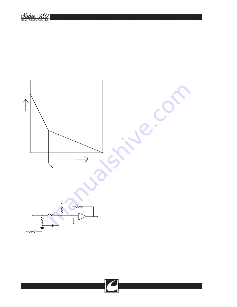
of VBASE at the low power settings. At lower
VDAC voltages, diode D5 becomes forward
biased so that R9 is essentially in parallel with
R26. Then the incremental gain is
(R32/R26+R32/R9). This steeper gain allows
VBASE to reach the voltage levels necessary for
the higher power settings. The voltage where the
gain slope changes is determined by the Thevenin
equivalent of +12V, R11, R10 (shown as Vth
and Rth in Figure 3.7) and R9.
R34 and R35 form a voltage divider to generate
a 5V offset for U21-3 to allow single supply
operation and to give a reference point for the
VSENSE and ISENSE voltages. When RFEN is
low U23-2 forces that voltage divider low, which
causes VBASE to turn off. A similar action occurs
when /WDTF goes low. R23 is summed into the
breakpoint amplifier to subtract out the effects of
the 5V on the non-inverting pin of the amplifier,
thus allowing the output of the base voltage gen-
erator to go to zero.
3.4.6 IFAIL and A.R.M. Analog Input
Refer to Figure 5.6b for the schematic containing
the IFAIL DAC A3U19. The output of this 8-bit
DAC (2.55 Vdc maximum output voltage) is fed
into the reference input of U23-9. The DAC is
controlled by the microprocessor to produce a
reference voltage for each mode of operation and
power setting. The ISENSE signal (refer to
Section 3.4.5 for a description of ISENSE) is
voltage divided and lowpass filtered by R39,
R49, and C61. Whenever the resulting voltage
exceeds the reference input voltage provided by
the DAC U19, a /IFAIL alarm is generated,
warning the microprocessor that the RF power
amplifier current is exceeding the maximum
allowed for that particular output mode and
power setting. This is a fatal alarm that produces
a "HLP - 5" code and shuts down the ESU.
Although it is possible for this to occur because
of a temporary fault condition and may be recov-
erable by cycling power, it generally occurs
because of a component failure in the Power Amp
circuitry.
Note that the same DAC is used for the A.R.M.
circuitry approximately every 12 milliseconds for
about 200 microseconds. During that time, the
microprocessor ignores /IFAIL since the reference
voltage provided by the DAC is being used to
provide a signal for the ARMCOMP comparator.
See Section 3.2.2 for a more detailed explanation
of the A.R.M. circuitry.
3.4.7 Waveform Generator
Refer to Figure 5.6b. A3U18 is a 32K x 8
EPROM that stores the bit patterns for the wave-
forms that drive the RF power amplifier. The
EPROM is arranged so that the upper address
slope=-R32(1/R26+1/R9)
slope=-R32/R26
Vout
Vdac
Vbreak=-(R9/Rt)*(Vt-5)+5-Vd
VDAC
VTH
RTH
10.0K
D4
1N4148
R9
20.0K
D5
1N4148
R26
56.2K
+12
R23
84.5K
R32
28.7K
+5
2
3
-
+
1
U21
LM324
VOUT
Figure 3.6 Base Voltage Generator
Transfer Curve
Figure 3.7 Basic Inverting Break
Point Amplifier
Summary of Contents for sabre 180
Page 1: ...Service Manual...
Page 6: ...This page intentionally left blank...