


Chapter 7: Register Descriptions
7–11
PCI Express Avalon-MM Bridge Control Register Access Content
June 2012
Altera Corporation
Stratix V Hard IP for PCI Express
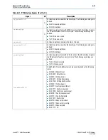
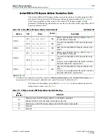
Table 7–22
defines the
Correctable Internal Error Mask
register. This register
controls which errors are forwarded as Internal Correctable Errors. This register is for
debug only.
S
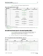
PCI Express Avalon-MM Bridge Control Register Access Content
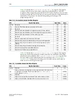
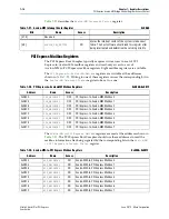
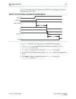
Control and status registers in the PCI Express Avalon-MM bridge are implemented
in the CRA slave module. The control registers are accessible through the Avalon-MM
slave port of the CRA slave module. This module is optional; however, you must
include it to access the registers.
The control and status register address space is 16 KBytes. Each 4-KByte sub-region
contains a set of functions, which may be specific to accesses from the PCI Express
Root Complex only, from Avalon-MM processors only, or from both types of
processors. Because all accesses come across the interconnect fabric—requests from
the Avalon-MM Stratix V Hard IP for PCI Express are routed through the interconnect
fabric—hardware does not enforce restrictions to limit individual processor access to
specific regions. However, the regions are designed to enable straight-forward
enforcement by processor software.
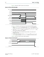
illustrates accesses to the Avalon-MM
control and status registers from the Host CPU and PCI Express link.
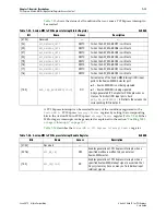
Table 7–22. Correctable Internal Error Mask Register
Bits
Register Description
Reset Value
Access
[31:7]
Reserved.
0
RO
[6]
Mask for Corrected Internal Error reported by the Application Layer.
1
RWS
[5]
Mask for configuration error detected in CvP mode.
0
RWS
[4:2]
Reserved.
0
RO
[1]
Mask for retry buffer correctable ECC error.
1
RWS
[0]
Mask for RX Buffer correctable ECC error.
1
RWS
Figure 7–1. Accesses to the Avalon-MM Bridge Control and Status Registers
Transaction,
Data Link,
and PHY
Q
sys Gene
r
a
t
ed Endpoin
t
(Al
t
e
r
a FPGA)
PCI Exp
r
ess Avalon-MM B
r
idge
Interconnect
Avalon-MM S
tr
a
t
ix V Ha
r
d IP fo
r
PCI Exp
r
ess
Con
tr
ol and S
t
a
t
us Regis
t
e
r
s
Con
tr
ol Regis
t
e
r
Access (CRA)
PCIe TLP Address
RX
PCIe
Link
0x0000-0x0FFF: PCIe processors
0x1000-0x1FFF: Addr translation
0x2000-0x2FFF: Reserved
0x3000-0x3FFF: Avalon-MM processors
Host
CPU
Avalon-MM
32-Bit Byte Address
Avalon-MM Slave