background image

Chapter 2

2-159

System Verification and Performance Tests

Agilent 8753ES Performance Test Records

Agilent Technologies Company
Model 8753ES

Serial Number

Report Number

Date

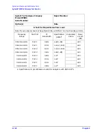
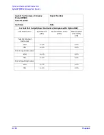
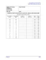
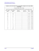
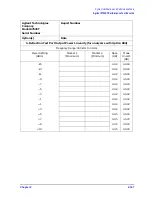
15. Harmonic Measurement Accuracy (Option 002 only)

Note: If your analyzer does not have Option 006, write “N/A” in all entries above 3 GHz.

Analyzer

Freq. 

(Fund.)

Ext. 

Source

Freq. 

(Harm.)

Power

Meter
Meas.

Cable

Loss

(A)

Power

Meter +

Cable

Loss

(B)

Network

Analyzer

Reading

(A 

 B) 

Harm. 

Meas. 

Accy.

Spec.

(dB)

Meas.

Uncert. 

(dB)

20 MHz

40 MHz

± 

1.5

± 

0.17

20 MHz

60 MHz

± 

1.5

± 

0.17

100 MHz

200 MHz

± 

1.5

± 

0.17

100 MHz

300 MHz

± 

1.5

± 

0.17

300 MHz

600 MHz

± 

1.5

± 

0.17

300 MHz

900 MHz

± 

1.5

± 

0.17

500 MHz

1 GHz

± 

1.5

± 

0.17

500 MHz

1.5 GHz

± 

1.5

± 

0.17

1 GHz

2 GHz

± 

1.5

± 

0.17

1 GHz

3 GHz

± 

1.5

± 

0.17

2 GHz

4 GHz

± 

3

± 

0.17

2 GHz

6 GHz

± 

3

± 

0.17

3 GHz

6 GHz

± 

3

± 

0.17

Summary of Contents for 8753ES

Page 1: ...Service Guide Agilent Technologies 8753ET ES Network Analyzers Agilent Part Number 08753 90484 Printed in USA June 2002 Supersedes February 2001 Copyright 1999 2002 Agilent Technologies Inc ...

Page 2: ...D WARRANTIES OF MERCHANTABILITY AND FITNESS FOR A PARTICULAR PURPOSE AGILENT SHALL NOT BE LIABLE FOR ERRORS OR FOR INCIDENTAL OR CONSEQUENTIAL DAMAGES IN CONNECTION WITH THE FURNISHING USE OR PERFORMANCE OF THIS DOCUMENT OR ANY INFORMATION CONTAINED HEREIN SHOULD AGILENT AND THE USER HAVE A SEPARATE WRITTEN AGREEMENT WITH WARRANTY TERMS COVERING THE MATERIAL IN THIS DOCUMENT THAT CONFLICT WITH THE...

Page 3: ...ure which if not correctly performed or adhered to could result in injury or loss of life Do not proceed beyond a warning note until the indicated conditions are fully understood and met CAUTION Caution denotes a hazard It calls attention to a procedure that if not correctly performed or adhered to would result in damage to or destruction of the instrument Do not proceed beyond a caution sign unti...

Page 4: ...s menu maps and key definitions The Programmer s Guide provides general GPIB programming information a command reference and example programs The Programmer s Guide contains a CD ROM with example programs The CD ROM provides the Installation and Quick Start Guide the User s Guide the Reference Guide and the Programmer s Guide in PDF format for viewing or printing from a PC The Service Guide provid...

Page 5: ... Verification and Performance Tests Introduction 2 2 System Specifications 2 2 Instrument Specifications 2 2 System Verification Procedure 2 3 Performance Tests 2 3 Certificate of Calibration 2 4 Agilent 8753ES System Verification and Performance Tests 2 5 System Verification Cycle and Kit Recertification 2 5 8753ES System Verification 2 5 8753ES Performance Tests 2 13 1 Test Port Output Frequency...

Page 6: ...ons 3 6 Source Default Correction Constants Test 44 3 7 Source Pretune Default Correction Constants Test 45 3 8 Analog Bus Correction Constants Test 46 3 9 Source Pretune Correction Constants Test 48 3 10 RF Output Power Correction Constants Test 47 3 11 Required Equipment and Tools 3 11 IF Amplifier Correction Constants Test 51 3 14 Required Equipment and Tools 3 14 ADC Offset Correction Constant...

Page 7: ...nce and FM Sideband Adjustment 3 56 Sequence Contents 3 56 4 Start Troubleshooting Here Assembly Replacement Sequence 4 3 Having Your Analyzer Serviced 4 4 Step 1 Initial Observations 4 5 Initiate the Analyzer Self Test 4 5 Step 2 Operator s Check 4 6 Description 4 6 Required Equipment and Tools 4 7 Procedure 4 7 Step 3 GPIB Systems Check 4 8 If Using a Plotter or Printer 4 8 If Using an External ...

Page 8: ... Line Voltage Selector Switch and Fuse 5 7 If the Red LED of the A15 Is ON 5 8 Check the A8 Post Regulator 5 8 Verify the A15 Preregulator 5 10 Check for a Faulty Assembly 5 11 Check the Operating Temperature 5 12 Inspect the Motherboard 5 12 If the Green LEDs of the A8 Are Not All ON 5 13 Remove A8 Maintain A15W1 Cable Connection 5 13 Check the A8 Fuses and Voltages 5 13 Remove the Assemblies 5 1...

Page 9: ...Correction Constants Test 44 7 5 2 RF Output Power Correction Constants Test 47 7 5 3 Sampler Magnitude and Phase Correction Constants Test 53 7 5 Phase Lock Error 7 6 Phase Lock Loop Error Message Check 7 6 A4 Sampler Mixer Check 7 8 A3 Source and A11 Phase Lock Check 7 8 A12 Reference Check 7 12 A13 A14 Fractional N Check 7 20 A7 Pulse Generator Check 7 25 A11 Phase Lock Check 7 28 Source Group ...

Page 10: ...6 Firmware Revision Softkey 10 41 GPIB Service Mnemonic Definitions 10 42 Invoking Tests Remotely 10 42 Analog Bus Codes 10 43 Error Messages 10 44 11 Error Terms Error Terms 11 2 Error Terms Can Also Serve a Diagnostic Purpose 11 3 Error Correction 11 4 Error Term Inspection 11 4 Error Term Descriptions 11 5 12 Theory of Operation How the Analyzer Works 12 3 The Built In Synthesized Source 12 3 T...

Page 11: ...ormation 13 5 Replaceable Part Listings 13 7 8753ET Major Assemblies Top 13 10 8753ES Major Assemblies Top 13 12 8753ET Major Assemblies Bottom 13 14 8753ES Major Assemblies Bottom 13 15 8753ES Option 014 Major Assemblies and Cables Bottom 13 16 8753ET Cables Top 13 18 8753ES Cables Top 13 20 8753ES Option 014 Cables Top 13 22 8753ET Cables Bottom 13 24 8753ES Cables Bottom 13 26 8753ET Cables Fro...

Page 12: ... Board Assembly A16 14 16 A3 Source Assembly 14 18 A4 A5 A6 Samplers and A7 Pulse Generator 14 20 A8 A10 A11 A12 A13 A14 Card Cage Boards 14 22 A9 CPU Board 14 24 A9BT1 Battery 14 26 A15 Preregulator 14 28 A17 Motherboard Assembly 14 30 A19 Graphics Processor 14 34 A20 Disk Drive Assembly 14 36 A20 Disk Drive Assembly Replacement 14 38 Test the disk eject function and adjust if required 14 39 Rein...

Page 13: ...t Markings 15 5 Lithium Battery Disposal 15 5 Safety Considerations 15 6 Safety Earth Ground 15 6 Before Applying Power 15 6 Servicing 15 7 General 15 8 Compliance with German FTZ Emissions Requirements 15 8 Compliance with German Noise Requirements 15 8 ...

Page 14: ...Contents xiv Contents ...

Page 15: ...1 1 1 Service Equipment and Analyzer Options ...

Page 16: ... T 20 and T 25 TORX screwdrivers Flat blade screwdrivers small medium and large 5 16 inch open end wrench for SMA nuts 2 mm extended bit Allen wrench 3 16 5 16 and 9 16 inch hex nut drivers 5 16 inch open end torque wrench set to 10 in lb 2 5 mm hex key driver Non conductive and non ferrous adjustment tool Needle nose pliers Tweezers Antistatic work mat with wrist strap 0 Phillips Screwdriver ...

Page 17: ... or E4418A E4419A A P T Power Sensor Frequency 300 kHz 3 GHz 8482A A P T Power Sensor for Option 006 Frequency 3 GHz 6 GHz 8481A A P T Photometer Tektronix J16 A Photometer Probe Tektronix J6503 A Light Occluder Tektronix 016 0305 00 A Printer HP ThinkJet DeskJet LaserJet P Floppy Disk one 3 5 inch formatted 1 44 MB any A Calibration Kit Type N 50Ω No substitute 85032B A P Calibration Kit 7 mm 50Ω...

Page 18: ... Set APC 7 50 Ω 11857D P A RF Cable 24 inch Type N 50 Ω 8120 4781 A P RF Cable Set Type N 50 Ω 11851B A GPIB Cable 10833A A P Coax Cable BNC m to BNC m 50Ω 10503A A Coax Cable BNC 8120 1840 A a P Performance Tests A Adjustments T Troubleshooting Table 1 1 Agilent 8753ET Service Test Equipment Required Equipment Critical Specifications HP Agilent Recommended Model Usea ...

Page 19: ...Power Sensor for Option 006 Frequency 3 GHz 6 GHz 8481A A P T Power Sensor for Option 075 Frequency 300 kHz 3 GHz 75Ω 8483A Opt H03 A P Photometer Tektronix J16 A Photometer Probe Tektronix J6503 A Light Occluder Tektronix 016 0305 00 A Printer HP ThinkJet DeskJet LaserJet P Floppy Disk one 3 5 inch formatted 1 44 MB any A Calibration Kit 7 mm 50Ω No substitute 85031B P Calibration Kit Type N 75Ω ...

Page 20: ... N f 1250 1477 P Adapter Type N f to Type N f 1250 0777 P Adapter Type N f to Type N f 75Ω 1250 1529 P RF Cable Set APC 7 50 Ω 11857D A P RF Cable 2 24 inch APC 7 50 Ω 2 8120 4779 A P RF Cable for Option 075 24 inch Type N 75Ω 8120 2408 A P RF Cable 24 inch Type N 50 Ω 8120 4781 A P GPIB Cable 10833A A P Coax Cable BNC m to BNC m 50Ω 10503A A Coax Cable BNC 8120 1840 A P a P Performance Tests A Ad...

Page 21: ...r care Table 1 3 Connector Care Quick Reference Handling and Storage Do Keep connectors clean Do Not Touch mating plane surfaces Extend sleeve or connector nut Set connectors contact end down Use plastic end caps during storage Visual Inspection Do Inspect all connectors carefully Do Not Use a damaged connector ever Look for metal particles scratches and dents Connector Cleaning Do Try compressed ...

Page 22: ... domain response It shows the response of a test device as a function of time or distance Displaying the reflection coefficient of a network versus time determines the magnitude and location of each discontinuity Displaying the transmission coefficient of a network versus time determines the characteristics of individual transmission paths Time domain operation retains all accuracy inherent with t...

Page 23: ...Handles This option is a rack mount kit containing a pair of flanges and the necessary hardware to mount the instrument with handles detached in an equipment rack with 482 6 mm 19 inches horizontal spacing Option 1CP Rack Mount Flange Kit with Handles This option is a rack mount kit containing a pair of flanges and the necessary hardware to mount the instrument with handles attached in an equipmen...

Page 24: ... to Agilent warranty for a total of a five year return to Agilent service warranty Option W51 This option replaces the standard warranty with a five year on site service warranty This option may not be available in all areas Option W32 This option provides for the annual return of your analyzer to Agilent for a commercial calibration for a period of three years The calibration provided is traceabl...

Page 25: ...If the previous service and support options were not purchased along with the analyzer there are many other repair and calibration options available from Agilent Technologies support organization These options cover a range of on site services and agreements with varying response times as well as return to Agilent agreements and per incident pricing Contact your local Agilent Technologies sales an...

Page 26: ...1 12 Chapter1 Service Equipment and Analyzer Options Service and Support Options ...

Page 27: ...2 1 2 System Verification and Performance Tests ...

Page 28: ...sed System specifications are expressed in two ways residual errors of the measurement system graphs of measurement uncertainty versus reflection and transmission coefficients System specifications are applicable when the measurement system is used to make error corrected measurements System specifications are verified in one of the following ways Complete the system verification procedure in this...

Page 29: ...measured with error correction applied These measurements are compared to measurement data stored on a unique serial numbered data disk included with the verification kit The measurement system passes the system verification procedure if the measurements of the test devices differ from the measurement data on the data disk by less than specified test limits The test limits account for the specifie...

Page 30: ...ormance tests are used to confirm instrument specifications the certificate of calibration will not include a system attachment The equipment and measurement standards used for the tests must be certified and must be traceable to recognized standards NOTE If you have a measurement application that does not use all of the measurement capabilities of the analyzer you may ask your local Agilent Techn...

Page 31: ...perating and Service Manual for more information NOTE The system verification procedures can also apply to analyzers with Option 075 75 ohm analyzers if minimum loss pads and type N m to APC 7 adapters are used Check to see how the verification kit floppy disk is labeled If your verification disk is labeled HP Agilent 8753D HP Agilent 8753E HP Agilent 8753ES HP Agilent 8753ET Verification Data Dis...

Page 32: ...ry you may wish to rename the file Press enter the desired name and press e Repeat steps a through d for each instrument state that you wish to save 2 To clear all internal memory press 3 Connect the equipment as shown in Figure 2 1 Let the system warm up for 30 minutes Description HP Agilent Model Number Calibration Kit 7 mm 85031B Verification Kit 7 mm 85029B Test Port Extension Cable Set 7 mm 1...

Page 33: ...n procedure 8 Position the paper in the printer so that printing starts at the top of the page 9 If you have difficulty with the printer If the interface on your printer is GPIB verify that the printer address is set to 1 or change the setting in the analyzer to match the printer If the interface on your printer is serial or parallel be sure that you selected the printer port and the printer type ...

Page 34: ...rt combination to reference test port 1 18 Press 19 When the analyzer finishes measuring the standard connect the 50 ohm termination supplied in the calibration kit to reference test port 1 20 Press 21 When the analyzer finishes measuring the standard connect the OPEN end of the open short combination to reference test port 2 22 Press 23 When the analyzer finishes measuring the standard connect th...

Page 35: ...alyzer internal memory press the following Rotate the knob to select Register 1 REG1 on the display Then press IMPORTANT Step 31 is crucial to the correct recall of the calibration during subsequent measurements The calibration MUST be stored in Register 1 REG1 of to be properly recalled 32 When the analyzer finishes saving the instrument state press Device Verification 1 Press 2 At the prompt con...

Page 36: ...er measures all S parameters magnitude and phase without pausing Also the analyzer only displays and prints the PASS FAIL information for the S parameter measurements that are valid for system verification Figure 2 4 Connections for the 20 dB Verification Device 4 When the analyzer finishes all the measurements connect the 50 dB attenuator supplied in the verification kit as shown in Figure 2 5 Fi...

Page 37: ...tch to reference test port 1 Figure 2 6 Mismatch Device Verification Setup 1 7 Press 8 When the analyzer finishes all the measurements connect the mismatch verification device as shown in Figure 2 7 Notice that Port B is now connected to reference test port 1 Figure 2 7 Mismatch Device Verification Setup 2 9 Press 10 You have completed the system verification procedure when the analyzer displays V...

Page 38: ...he calibration by pressing c Use the front panel knob to highlight the calibration you want to recall and press d Connect the short to reference test port 1 e Press f Press g Check that the trace response is 0 00 0 05 dB h Disconnect the short and connect it to reference test port 2 i Press j Check that the trace response is 0 00 0 05 dB k If any of the trace responses are out of the specified lim...

Page 39: ...put Power Level Accuracy on page 2 19 4 Test Port Output Power Linearity on page 2 22 5 Minimum R Channel Level on page 2 28 6 Test Port Input Noise Floor Level on page 2 32 7 Test Port Input Frequency Response on page 2 36 8 Test Port Crosstalk on page 2 45 9 Uncorrected Port Performance on page 2 50 10 System Trace Noise on page 2 56 11 Test Port Receiver Magnitude Dynamic Accuracy on page 2 59 ...

Page 40: ... up time 30 minutes Specifications Required Equipment Procedure 1 Connect the equipment as shown in Figure 2 8 Frequency Range Frequency Accuracya a At 25 C 5 C 30 kHz to 3 GHz 10 ppm 3 GHz to 6 GHzb b Only for analyzers with Option 006 10 ppm Description HP Agilent Part or Model Number Frequency Counter 5350B 51B 52B Cable 50Ω Type N 24 inch 8120 4781 Adapter APC 3 5 f to Type N f 1250 1745 Adapt...

Page 41: ...and Performance Tests Figure 2 8 Test Port Output Frequency Range and Accuracy Test Setup 2 Press 3 Press and write the frequency counter reading on the performance test record 4 Repeat step 3 for each instrument frequency listed in the performance test record Preset Sweep Setup CW FREQ 30 k m ...

Page 42: ...cy of the counter used 2 If the analyzer fails by a significant margin at all frequencies especially if the deviation increases with frequency the master time base probably needs adjustment In this case refer to Frequency Accuracy Adjustment on page 3 43 The Fractional N Frequency Range Adjustment on page 3 40 also affects frequency accuracy 3 Refer to Chapter 7 Source Troubleshooting for related ...

Page 43: ...e lock conditions are confirmed at a power level of 25 dBm Analyzer warm up time 30 minutes Specifications Required Equipment Procedure 1 Set the external source to a CW frequency of 10 MHz and power level of 25 dBm 2 Connect the equipment as shown in Figure 2 9 Figure 2 9 External Source Mode Frequency Range Test Setup Frequency Range 300 kHz to 3 GHz 300 kHz to 6 GHza a Only for analyzers with O...

Page 44: ...d for the set CW signal 6 Set the external source to a CW frequency of 20 MHz 7 On the analyzer press or the next external source frequency 8 Repeat steps 5 through 7 for the other external source CW frequencies listed in the performance test record In Case of Difficulty If the analyzer displayed any phase lock error messages 1 Be sure the external source power is set to 25 dBm 2 Make sure the ana...

Page 45: ...inutes Specifications Required Equipment Procedure 1 Zero and calibrate the power meter For more information of how to perform this task refer to the power meter operating manual 2 Connect the equipment as shown in Figure 2 10 Frequency Range Test Port Output Power Accuracya a At 0 dBm and 25 C 5 C 300 kHz to 3 GHz 1 0 dB 3 GHz to 6 GHzb b Only for analyzers with Option 006 1 0 dB Description HP A...

Page 46: ...ctory preset test port power is 0 dBm 4 Press Set the calibration factor on the power meter for this CW frequency 5 Write the power meter reading on the performance test record 6 Repeat steps 4 and 5 for each CW frequency listed in the performance test record For analyzers with Option 006 use the HP Agilent 8481A power sensor for all frequencies above 3 GHz Preset Sweep Setup CW FREQ 300 k m ...

Page 47: ...n and Performance Tests In Case of Difficulty 1 Be sure the source power is switched on Press Check the softkey ON should be highlighted Otherwise press to switch on the source power 2 Refer to Chapter 7 Source Troubleshooting for more troubleshooting information Power SOURCE PWR SOURCE PWR ...

Page 48: ...perator s Check on page 4 6 Analyzer warm up time 30 minutes Specifications Required Equipment Power Range Power Level Linearitya a Relative to 0 dBm from 300 kHz to 3 GHz 2 GHz for Option 075 6 GHz for Option 006 15 to 5 dBm 0 2 dB 5 to 10 dBm 0 5 dB 5 to 8 dBmb b Options 014 and 075 0 5 dB Description HP Agilent Part or Model Number Power Meter 437A 438A or E4418B 4419B Power Sensor 8482A Adapte...

Page 49: ...rate the power meter for the HP Agilent 8482A power sensor 2 Connect the equipment as shown in Figure 2 11 Figure 2 11 Setup for Power Meter Calibration on Test Port 1 3 Press 4 Press 5 Press then If the analyzer has Option 075 press If the analyzer has Option 006 press Preset Avg IF BW 100 x1 Sweep Setup NUMBER of POINTS 51 x1 Start 300 k m Stop 2 G n Stop 3 G n ...

Page 50: ...ion factor data points The following softkeys are included in the sensor calibration factor entries menu press to select a point where you can use the front panel knob or entry keys to enter a value press to edit or change a previously entered value press to delete a point from the sensor calibration factor table select this key to add a point into the sensor calibration factor table select this k...

Page 51: ... panel knob to point to the data point you want to modify and press 13 Press the appropriate softkeys to create a power sensor calibration factors table 14 Press to exit the sensor calibration factor entries menu 15 Press to start the power meter calibration NOTE The analyzer displays the PC annotation indicating the power meter calibration is active Output Power Linearity Measurement 300 kHz to 3...

Page 52: ...two sections Power Meter Calibration from 3 GHz to 6 GHz Option 006 only 1 Disconnect the 8482A power sensor from the power meter and connect the 8481A power sensor in its place Zero and calibrate the power meter for this sensor Connect the equipment as shown in Figure 2 11 on page 2 23 using the 8481A sensor 2 Press 3 Press 4 Press Press the appropriate keys to build a sensor calibration factor t...

Page 53: ...uld be within the specified range for each power level with reference to the fixed marker value 12 This completes the test If you have problems with this test go to In Case of Difficulty next In Case of Difficulty 1 Ensure that the power meter and power sensors are operating to specifications Be sure to set the power meter calibration factor for the range of frequencies that you are testing 2 Veri...

Page 54: ...hase lock conditions Analyzer warm up time 30 minutes Specifications Required Equipment Procedure 1 Connect the equipment as shown in Figure 2 13 Figure 2 13 Minimum R Channel Level Test Setup Frequency Range Minimum R Channel Level 300 kHz to 3 GHz 35 dBm 3 GHz to 6 GHza a Only for analyzers with Option 006 30 dBm Description HP Agilent Part or Model Number Adapter APC 3 5 m to APC 7 1250 1746 Ca...

Page 55: ...9 Write the test port power that is displayed on the analyzer on the performance test record 10 Repeat steps 5 through 9 for the other CW frequencies listed in the performance test record In Case of Difficulty 1 Check the flexible RF cable W8 as shown in Figure 2 14 between the R sampler assembly A4 and the phase lock assembly A11 Make sure it is connected between A11J1 PL IF IN and 1st IF Out CAU...

Page 56: ...ion 2 Using an ohmmeter verify that cable W8 is not open In addition examine both the cable connectors measure the resistance between the cable center pin and the cable connector and make sure it is not close to zero 3 Check the R sampler by substituting it with the B sampler A6 Do this by moving cable W8 to the B sampler A6 as shown in Figure 2 15 ...

Page 57: ...the test but select the B sampler A6 by pressing in step 2 Use the following specifications 300 kHz to 3 GHz 27 dBm 3 GHz to 6 GHz 22 dBm 6 If the analyzer fails the test replace the A11 assembly 7 Verify that the high low band adjustments are still within specifications For more information on how to perform this task refer to High Low Band Transition Adjustment on page 3 47 8 Refer to Chapter 7 ...

Page 58: ...F Bandwidth Average Noise Level for 50Ω analyzers Average Noise Level for 75Ω analyzers 300 kHz to 3 0 GHz Test Port 1 3 kHz 82 dBm 80 dBm 300 kHz to 3 0 GHz Test Port 1 10 Hz 102 dBm 100 dBm 300 kHz to 3 0 GHz Test Port 2 3 kHz 82 dBm 80 dBm 300 kHz to 3 0 GHz Test Port 2 10 Hz 102 dBm 100 dBm 3 0 GHz to 6 0 GHza a Only for analyzers with Option 006 Test Port 1 3 kHz 77 dBm N A 3 0 GHz to 6 0 GHz...

Page 59: ...62 µU the value that you would put in the equation is 62 10 6 7 Write this calculated value on the performance test record Test Port 1 Noise Floor Level from 300 kHz to 3 GHz IF BW 10 Hz 8 Press to change the IF bandwidth to 10 Hz 9 Press 10 When the analyzer finishes the sweep notice the mean value 11 Convert the measured linear magnitude mean value to log magnitude using this equation Power dBm ...

Page 60: ...nitude mean value to log magnitude using this equation Power dBm 20 log10 linear magnitude mean value 22 Write this calculated value on the performance test record 23 This completes the test port input noise floor level procedure if your analyzer does not have Option 006 If your analyzer has Option 006 continue with the next section Test Port 2 Noise Floor Level from 3 GHz to 6 GHz IF BW 3 kHz Opt...

Page 61: ...0 log10 linear magnitude mean value 38 Write this calculated value on the performance test record Test Port 1 Noise Floor Level from 3 GHz to 6 GHz IF BW 3 kHz Option 006 only 39 Press 40 Press 41 When the analyzer finishes the sweep notice the mean value 42 Convert the measured linear magnitude mean value to log magnitude using this equation Power dBm 20 log10 linear magnitude mean value 43 Write...

Page 62: ...tion for Test Port 1 from 300 kHz to 3 GHz 1 Zero and calibrate the power meter for the 8482A sensor 2 Connect the equipment as shown in Figure 2 18 Frequency Range Input Frequency Responsea a At 0 dBm 300 kHz to 3 GHz 1 dB 3 GHz to 6 GHzb b Only for analyzers with Option 006 2 dB Description HP Agilent Part or Model Number Power Meter 436A 437B 438A or E4418B 4419B Power Sensor 8482A Cable APC 7 ...

Page 63: ...correct power meter model Use the 438A 437 selection if the power meter is an HP Agilent E4419B or an E4418B 7 Press The default power meter GPIB address is 13 Make sure it is the same as your power meter GPIB address Otherwise use the analyzer front panel keypad to enter the correct GPIB address for your power meter 8 Press Preset Avg IF BW 3 k m Start 300 k m Stop 3 G n Local SYSTEM CONTROLLER S...

Page 64: ...nt from the sensor calibration factor table select this key to add a point into the sensor calibration factor table select this key to erase the entire sensor calibration factor table select this key when done entering points to the sensor calibration factor table As an example the following are the keystrokes for entering the first two calibration factor data points for the 8482A power sensor ass...

Page 65: ...eep then continue with this procedure NOTE The analyzer displays the PC annotation indicating the power meter calibration is active Test Port 2 Input Frequency Response from 300 kHz to 3 GHz 16 Connect the equipment as shown in Figure 2 19 Figure 2 19 Test Port 2 Input Frequency Response Test Setup 17 Press 18 Press 19 Press to put marker 1 at the minimum magnitude location of the trace 20 Press t...

Page 66: ...equipment as shown Figure 2 20 Figure 2 20 Setup for Power Meter Calibration on Test Port 2 23 Press 24 Press to start the power meter calibration for test port 2 25 When the analyzer displays the message POWER METER CALIBRATION SWEEP DONE connect the equipment as shown as in Figure 2 21 Sweep Setup TRIGGER MENU CONTINUOUS Meas INPUT PORTS TESTPORT 2 Cal PWRMTR CAL ONE SWEEP TAKE CAL SWEEP ...

Page 67: ... 30 If your analyzer does not have Option 006 this completes the performance test If your analyzer has Option 006 continue with the next sections Power Meter Calibration for Test Port 2 from 3 GHz to 6 GHz Option 006 only 31 Replace the power sensor with the 8481A and then set up the power meter a Cycle the line power for the power meter b Zero and calibrate the power meter with the new sensor 32 ...

Page 68: ...he sensor calibration factor entries menu 37 To select the 8481A power sensor press Press 38 Press to start the power meter calibration Test Port 1 Input Frequency Response from 3 GHz to 6 GHz 39 When the analyzer finishes the calibration sweep connect the equipment as shown in Figure 2 23 Figure 2 23 Setup for Test Port 1 Input Frequency Response Start 3 G n Stop 6 G n Cal PWRMTR CAL LOSS SENSR L...

Page 69: ...Hz to 6 GHz Option 006 only 44 Connect the equipment as shown in Figure 2 24 Figure 2 24 Setup for Power Meter Calibration on Test Port 1 45 Press 46 Press to start the power meter calibration for test port 1 Test Port 2 Input Frequency Response from 3 GHz to 6 GHz Option 006 only 47 When the analyzer displays the message POWER METER CALIBRATION SWEEP DONE connect the equipment as shown as in Figu...

Page 70: ...tion of the trace 51 Write the marker 1 or marker 2 reading whichever has the largest absolute magnitude in the performance test record In Case of Difficulty 1 Be sure you have used the correct power sensor for the frequency range 2 Verify that the calibration factors that you have entered for the power sensors are correct 3 Repeat this test with a cable that is known to be good Meas INPUT PORTS B...

Page 71: ...en the analyzer s test ports 1 and 2 as shown in Figure 2 26 Use the appropriate cable for your analyzer 50Ω or 75Ω Frequency Range Crosstalka a Measurement conditions 25 C 5 C normalized to a through measured with two shorts or shielded open 10 Hz IF BW averaging factor 8 alternate mode source power at 10 dBm or 8 dBm for Option 014 or Option 075 300 kHz to 3 GHz 100 dB 3 GHz to 6 GHzb b Only for...

Page 72: ...ay 8 Press 9 Press 10 Press Wait for the sweep to finish as indicated by the Hld notation on the left side of the display 11 Press 12 Press 13 Press Preset Cal MORE ALTERNATE A and B Start 300 k m Stop 3 G n Sweep Setup NUMBER of POINTS 101 x1 Power 10 x1 8 x1 Avg IF BW 10 x1 Meas Trans FWD S21 B R Sweep Setup TRIGGER MENU SINGLE Display DATA MEMORY DATA MEM Chan 2 Meas Trans REV S12 A R Sweep Set...

Page 73: ...n on the left side of the display 7 Press 8 Write the marker value which appears on the analyzer display in the performance test record This completes the test If your analyzer has Option 006 proceed to the next section Normalization from 3 GHz to 6 GHz Option 006 only 1 Set up the equipment again as shown in Figure 2 26 on page 2 46 2 Press 3 Press Wait for the sweep to finish as indicated by the...

Page 74: ...nish as indicated by the Hld notation on the left side of the display 14 Press 15 Write the marker value which appears on the analyzer display in the performance test record In Case of Difficulty 1 Remove the instrument top cover Using an 8 lb inch torque wrench verify that all semirigid cables connected to the sampler mixer assemblies are tight In addition tighten any loose screws on the sampler ...

Page 75: ...Chapter 2 2 49 System Verification and Performance Tests Agilent 8753ES System Verification and Performance Tests Figure 2 28 8753ES Bottom View ...

Page 76: ...quired Equipment Procedure First Full 2 Port Calibration 1 Connect the equipment as shown in Figure 2 29 Uncorrecteda Error Terms a At 25 C 5 C with less than 1 C deviation from the measurement calibration temperature Frequency Range 300 kHz to 1 3 GHz 1 3 GHz to 3 GHz 3 GHz to 6 GHzb b Only for analyzers with Option 006 Directivity 35 dB 30 dB 25 dB Source Match 16 dB 16 dB 14 dB Load Match 18 dB...

Page 77: ...ion kit 10 Press 11 Connect the OPEN end of the open short combination to reference test port 2 12 Press 13 Connect the SHORT end of the open short combination to reference test port 2 14 Press 15 Connect the termination to the reference test port 2 16 Press 17 When the analyzer displays PRESS DONE IF FINISHED WITH STD s press Wait for the message COMPUTING CAL COEFFICIENTS to disappear from the a...

Page 78: ...cient 26 Press 27 When the analyzer finishes the test repeat steps 22 through 25 Transmission Tracking Reverse Calibration Coefficient 28 Press 29 When the analyzer finishes the test press 30 Using the front panel knob to move the marker along the data trace locate the maximum and minimum values for the 300 kHz to 1 3 GHz frequency range 31 Enter the data trace value that is of greater deviation f...

Page 79: ...as Option 075 40 Press 41 Connect the OPEN end of the open short combination supplied in the calibration kit to reference test port 1 42 Press 43 Connect the SHORT end of the open short combination to reference test port 1 44 Press 45 Replace the open short combination with the termination supplied in the calibration kit 46 Press 47 Connect the OPEN end of the open short combination to the analyze...

Page 80: ...32 Transmission Calibration Test Setup 55 Press 56 Press Load Match Forward Calibration Coefficient 57 Press 58 When the test is done press 59 Using the front panel knob locate the maximum value of the data trace for the 300 kHz to 1 3 GHz frequency range 60 Write the maximum value on the performance test record 61 Repeat the previous three steps for the other frequency ranges listed on the perfor...

Page 81: ...minimum values for the 300 kHz to 1 3 GHz frequency range 69 Enter the data trace value that is of greater deviation from zero into the performance test record This is the greater absolute value of either the maximum data trace value or the minimum data trace value 70 Repeat the previous three steps for the other frequency ranges listed on the performance test record Transmission Tracking Forward ...

Page 82: ...for a transmission measurement in CW mode using a through cable having 0 dB loss with the source set to 5 dBm and no averaging System Trace Noise Phasea IF Bandwidth 10 Hz 300 kHz to 3 GHz A R 0 001 dB rms 0 006 rms 300 kHz to 3 GHz B R 0 001 dB rms 0 006 rms 3 GHz to 6 GHz Option 006 A R 0 002 dB rms 0 012 rms 3 GHz to 6 GHz Option 006 B R 0 002 dB rms 0 012 rms IF Bandwidth 3 kHz 300 kHz to 3 GH...

Page 83: ...yzer display on the performance test record A R Trace Noise Phase IF BW 10 Hz 8 Press 9 Write the s dev value which appears on the analyzer display on the performance test record A R Trace Noise Phase IF BW 3 kHz 10 Press 11 Press Wait for the sweeps to finish as indicated by the Hld notation on the left side of the display 12 Write the s dev value on the performance test record Preset Power 5 x1 ...

Page 84: ...ide of the display 20 Write the s dev value on the performance test record B R Trace Noise Magnitude IF BW 10 Hz 21 Press 22 Write the s dev value on the performance test record Option 006 only 1 Press 2 Go back to A R Trace Noise Magnitude IF BW 10 Hz on page 2 57 and perform this entire procedure again Record all values in the performance test record under Test Frequency 6 GHz In Case of Difficu...

Page 85: ...nce Tests 11 Test Port Receiver Magnitude Dynamic Accuracy The analyzer s receiver linearity versus input power is measured with a calibrated step attenuator Measurement uncertainty is minimized by using the analyzer s capability to perform error correction Analyzer warm up time 30 minutes Specifications ...

Page 86: ...from 40 to 80 dB 0 025 dB from 80 to 90 dB 0 05 dB 90 dB The second calibration measurement characterizes match stability between attenuator settings for each attenuator port The vector difference of S11 or S22 between the reference attenuation step and all the other steps is measured The magnitude of this difference is certified to be 0 0316 30 dB Description HP Agilent Part or Model Number Power...

Page 87: ...w for the 10 dB 8496A setting c Continue transferring the remaining values of the 8496A attenuation errors to column B in Table 2 1 2 In Table 2 1 transfer the 10 dB error value located within the parenthesis in column B to each space in column C NOTE The 8496A used for this test will have known attenuator errors for attenuations up to 100 dB using a test frequency of 30 MHz The attenuation used a...

Page 88: ... error Calculate the values in this column by subtracting the values in column D from the values in column E The result is E D F 5 Transfer the values from column F in Table 2 1 to column F in the performance test record for both test ports Power Meter Calibration 6 Zero and calibrate the power meter Refer to the power meter manual for details on this procedure 7 Connect the equipment as shown in ...

Page 89: ...Chapter 2 2 63 System Verification and Performance Tests Agilent 8753ES System Verification and Performance Tests Figure 2 34 Power Meter Calibration for Magnitude Dynamic Accuracy ...

Page 90: ...if the power meter is an E4419B or E4418B d Select the calibration kit and enter the power sensor calibration data enter the power sensor calibration data for 30 MHz 11 Take a power meter calibration sweep 12 Verify that the power meter reads approximately 20 dBm Full 2 Port Calibration 13 Connect the equipment as shown in Figure 2 35 Preset Sweep Setup CW FREQ 30 M µ NUMBER of POINTS 51 x1 Power ...

Page 91: ...m Verification and Performance Tests Agilent 8753ES System Verification and Performance Tests Figure 2 35 Full 2 Port Calibration 14 Perform a full 2 port error correction with isolation using the HP Agilent 85031B cal kit ...

Page 92: ...ect the equipment as shown in Figure 2 36 Confirm that the step attenuator is set to 10 dB Figure 2 36 Magnitude Dynamic Accuracy Measurement 16 To set up the dynamic accuracy measurement press the following 17 Wait for the sweep to finish then press Meas Trans FWD S21 B R Marker Fctn MKR MODE MENU STATS ON Sweep Setup TRIGGER MENU SINGLE Display DATA MEMORY DATA MEM ...

Page 93: ...hich are abbreviations for 10 3 units 10 6 units and 10 9 units respectively 22 Repeat steps 19 through 21 for each setting of the step attenuator as written in the performance test record 23 For each pair of real and imaginary parts calculate the value given by the formula 10 log10 Real Part 2 Imaginary Part 2 Write the result in the performance test record in the Test Port Measurement column col...

Page 94: ...gilent 8753ES System Verification and Performance Tests Figure 2 37 Power Meter Calibration for Magnitude Dynamic Accuracy 27 Set the step attenuator to 10 dB 28 Set the following analyzer parameters Sweep Setup TRIGGER MENU CONTINUOUS Meas Trans REV S12 A R ...

Page 95: ...wer meter reads approximately 20 dBm Full 2 Port Calibration 31 Connect the equipment as shown in Figure 2 38 Figure 2 38 Full 2 Port Calibration 32 Perform a full 2 port error correction with isolation using the 85031B cal kit If necessary refer to your analyzer s user s guide for detailed information on performing calibrations Cal PWRMTR CAL 20 x1 ONE SWEEP TAKE CAL SWEEP ...

Page 96: ...acy 33 Connect the equipment as shown in Figure 2 39 Figure 2 39 Magnitude Dynamic Accuracy Measurement 34 Set the step attenuator to 10 dB 35 To set up the dynamic accuracy measurement press the following 36 Wait for the sweep to finish then press 37 Set the step attenuator to 0 dB Display DATA Sweep Setup TRIGGER MENU SINGLE Display DATA MEMORY DATA MEM ...

Page 97: ...nary Part 2 Write the result in the performance test record in the Test Port Measurement column column G 43 Calculate the dynamic accuracy for each attenuator setting by using the formula G F the absolute value of the difference between the values in column G and column F In Case of Difficulty 1 If the analyzer fails the test at all power levels be sure you followed the recommended attenuator sett...

Page 98: ...ted to avoid compression The attenuation is removed and compression is observed and measured Analyzer warm up time 30 minutes Specifications Required Equipment Procedure 1 Connect the equipment as shown in Figure 2 40 Figure 2 41 for 75Ω analyzers Frequency Range Magnitudea a With a 10 Hz IF bandwidth 300 kHz to 3 GHz 0 42 dB 3 GHz to 6 GHz 0 76 dB Description HP Agilent Part or Model Number Cable...

Page 99: ...mpression Test Setup Figure 2 41 Test Port Receiver Magnitude Compression for 75Ω Analyzers 2 On the analyzer press 3 Press 4 Press 5 Press or next CW frequency 6 Set the step attenuator to 20 dB attenuation Preset Avg IF BW 10 x1 Meas INPUT PORTS B Sweep Setup SWEEP TYPE MENU POWER SWEEP Start 10 x1 Marker 10 x1 MODE MENU REF 1 Sweep Setup CW FREQ 300 k m ...

Page 100: ...h CW frequency listed in the performance test record For step 14 record the values in the performance test record under Measured Value Test Port 1 In Case of Difficulty 1 If the analyzer fails test port 2 magnitude compression a Repeat this test b Replace the A6 B sampler assembly if the analyzer still fails the test 2 If the analyzer fails test port 1 magnitude compression a Repeat this test b Re...

Page 101: ...uation is removed and compression is observed and measured Analyzer warm up time 30 minutes Specifications Required Equipment for 50Ω Analyzers Procedure 1 Connect the equipment as shown in Figure 2 42 Figure 2 43 for 75Ω analyzers CW Frequency Test Port Phasea a With 10 Hz IF bandwidth 300 kHz to 3 GHz Test Port 1 6 3 GHz to 6 GHzb b Only for analyzers with Option 006 Test Port 1 7 2 Description ...

Page 102: ...2 Test Port Phase Compression Test Setup Figure 2 43 Test Port Phase Compression Test Setup for 75Ω Analyzers 2 Press 3 Press 4 Press 5 Press or next CW frequency Preset IF BW 10 x1 Meas INPUT PORTS B R Format PHASE Sweep Setup SWEEP TYPE MENU POWER SWEEP Start 10 x1 Marker 10 x1 MODE MENU REF 1 Sweep Setup CW FREQ 300 k m ...

Page 103: ...17 Repeat steps 5 through 14 for each CW frequency listed in the performance test record Record the entries under Measured Value Test Port 1 In Case of Difficulty 1 If the analyzer fails the test port 2 phase compression test a Repeat this test b Replace the A6 B sampler assembly if analyzer still fails the test 2 If the analyzer fails the test port 1 phase compression test a Repeat this test b Re...

Page 104: ... time 30 minutes NOTE The test port input 3rd harmonic specifications are better than the test port output 3rd harmonic specifications Specifications Required Equipment Test Port Harmonic Limit Output 2nd 25 dBc 10 dBma a 8 dBm for analyzers with Option 014 or 075 Output 3rd 25 dBc 10 dBma Input Port 1 2nd 15 dBc 8 dBm Input Port 1 3rd 30 dBc 8 dBm Input Port 2 2nd 15 dBc 8 dBm Input Port 2 3rd 30...

Page 105: ...10 Hz 4 Connect the equipment as shown in Figure 2 44 Figure 2 44 Test Port Output Harmonics Test Setup 5 Press 6 After one sweep press to normalize the trace 7 Press 8 After one sweep press to get a better viewing of the trace 9 Press 10 Write the marker 1 value which appears on the analyzer display on the performance test record This is the worst case test port output 2nd harmonic Preset Power 1...

Page 106: ...press 17 Press 18 Write the marker 1 value on the performance test record Test Port 1 Input Worst Case 2nd Harmonic 19 Connect the equipment as shown in Figure 2 45 Figure 2 45 Receiver Harmonics Test Setup 20 Press 21 Press 22 To set the frequency range press If you do not have Option 006 press If you have Option 006 press Stop 1 G n Stop 2 G n System HARMONIC MEAS HARMONIC OFF Display DATA MEMOR...

Page 107: ...s Test Port 2 Input Worst Case 2nd Harmonic 38 To set the stop frequency for measuring the 2nd harmonic If you do not have Option 006 press If you have Option 006 press 39 Press 40 After one sweep press to normalize the trace 41 Press 42 After one sweep press to get a better viewing of the trace 43 Press 44 Write the marker 1 value which appears on the analyzer display on the performance test reco...

Page 108: ...have Option 006 press If you have Option 006 press 46 Press 47 After one sweep press to normalize the trace 48 Press to get a better viewing of the trace 49 Press 50 After one sweep press 51 Press 52 Write the marker 1 value on the performance test record Stop 1 G n Stop 2 G n System HARMONIC MEAS HARMONIC OFF Display DATA MEMORY DATA MEM Scale Ref AUTO SCALE System HARMONIC MEAS HARMONIC THIRD Sc...

Page 109: ... Specifications Required Equipment Procedure Determine the Cable Loss at Specified Frequencies 1 Connect the equipment as shown in Figure 2 46 Observe the differences between the standard 8753ES and the Option 075 75Ω 8753ES Frequency Range Accuracy 16 MHz to 3 GHz 1 5 dB 3 GHz to 6 GHza a Only for analyzers with Option 006 3 0 dB Description HP Agilent Part or Model Number External Source 83712B ...

Page 110: ...ss 3 Press 4 Disconnect the cable from Test Port 2 Connect the type N f to type N f adapter to the end of the cable and attach the second type N cable as shown in Figure 2 47 Figure 2 47 Harmonic Measurement Accuracy Cable Loss Setup 2 5 Press 6 Press Preset Start 40 M µ Meas Trans S21 B R Cal CALIBRATE MENU RESPONSE THRU Scale Ref SCALE DIV 1 x1 Sweep Setup TRIGGER MENU SINGLE ...

Page 111: ...meter for the 8482A power sensor 9 Set up the equipment as shown in Figure 2 48 For the type N cable use the one that was added in step 4 10 On the analyzer press 11 On the external source set the power level for 6 dBm Figure 2 48 Harmonic Measurement Accuracy Test Setup Harmonic Measurement Accuracy 12 On the analyzer press Then press or the next fundamental frequency for the network analyzer 13 ...

Page 112: ...e power meter set the cal factor appropriate for the frequency of the external source Record the power meter reading in the performance test record under Power Meter Meas for 60 MHz or the next third harmonic frequency 19 Repeat steps 12 through 18 for the fundamental second and third harmonic frequencies Before measuring harmonics above 3 GHz zero and calibrate the power meter using the 8481A pow...

Page 113: ...n Check to see how the verification kit floppy disk is labeled If your verification disk is labeled HP Agilent 8753D HP Agilent 8753E HP Agilent 8753ES or HP Agilent 8753ET Verification Data Disk you may proceed with the system verification If your verification disk is not labeled as indicated above you may send your HP Agilent 85029B 7 mm verification kit to the nearest service center for recerti...

Page 114: ... d If the instrument state file was not saved to disk with the same name that it had while in internal memory you may wish to rename the file Press enter the desired name and press e Repeat steps a through d for each instrument state that you wish to save To clear all internal memory press 2 Connect the equipment as shown in Figure 2 49 Let the system warm up for 30 minutes Figure 2 49 System Veri...

Page 115: ...nge the setting in the analyzer to match the printer If the interface on your printer is serial or parallel be sure that you selected the printer port and the printer type correctly Refer to the analyzer s user s guide for more information on how to perform these tasks 9 Press 10 When the analyzer displays Sys Ver Init DONE the initialization procedure is complete CAUTION Do not press or recall an...

Page 116: ...mbination to reference test port 1 18 Press 19 When the analyzer finishes measuring the standard connect the 50 ohm termination supplied in the calibration kit to reference test port 1 20 Press 21 When the analyzer finishes measuring the standard press 22 Remove the 50 ohm termination from reference test port 1 and connect both reference test ports together as shown in Figure 2 51 Figure 2 51 Tran...

Page 117: ... each measurement Press after each measurement If you switched the record function on the analyzer takes all the required measurements for the test without pausing Also the analyzer only displays and prints the PASS FAIL information for the measurements that are valid for system verification Figure 2 52 Connections for the 20 dB Verification Device 30 When the analyzer finishes all the measurement...

Page 118: ...ice with the verification mismatch as shown in Figure 2 54 Be sure that you connect Port A of the verification mismatch to reference test port 1 Figure 2 54 Mismatch Device Verification Setup 1 33 Press 34 When the analyzer finishes all the measurements connect the mismatch verification device as shown in Figure 2 55 Notice that Port B is now connected to reference test port 1 29 x1 EXECUTE TEST C...

Page 119: ...ess Using the front panel knob highlight the title of the enhanced response calibration that you did earlier then press 3 Repeat the Device Verification procedure 4 If the analyzer still fails the test check the measurement calibration as follows a Press b Recall the calibration by pressing c Use the front panel knob to highlight the calibration you want to recall and press d Connect the short to ...

Page 120: ...ion and Performance Tests g Check that the trace response is 0 00 0 05 dB h If the trace response is out of the specified limits repeat the Enhanced Response Calibration and Device Verification procedures 5 Refer to Chapter 4 Start Troubleshooting Here for more troubleshooting information ...

Page 121: ...n page 2 96 2 External Source Mode Frequency Range on page 2 98 3 Reflection Test Port Output Power Level Accuracy on page 2 100 4 Reflection Test Port Output Power Linearity Analyzers without Option 004 on page 2 102 5 Reflection Test Port Output Power Linearity Analyzers with Option 004 on page 2 108 6 Minimum R Channel Level on page 2 114 7 Transmission Test Port Input Noise Floor Level on page...

Page 122: ...e the analyzer s output frequency Analyzer warm up time 30 minutes Specifications Required Equipment Procedure 1 Connect the equipment as shown in Figure 2 56 Figure 2 56 Reflection Test Port Output Frequency Range and Accuracy Frequency Range Frequency Accuracya a At 25 C 5 C 300 kHz to 3 GHz 10 ppm 3 GHz to 6 GHzb b Only for analyzers with Option 006 10 ppm Description HP Agilent Part or Model N...

Page 123: ...ency is close to the specification limits check the time base accuracy of the frequency counter used 2 If the analyzer fails by a significant margin at all frequencies especially if the deviation increases with frequency the master time base probably needs adjustment In this case refer to the Frequency Accuracy Adjustment on page 3 43 The Fractional N Frequency Range Adjustment on page 3 40 also a...

Page 124: ...fications Required Equipment Procedure 1 Set the external source for a CW frequency of 10 MHz and power level of 25 dBm 2 Connect the equipment as shown in Figure 2 57 Figure 2 57 External Source Mode Frequency Range Test Setup 3 On the network analyzer press Frequency Range 300 kHz to 3 GHz 300 kHz to 6 GHza a Only for analyzers with Option 006 Description HP Agilent Part or Model Number External...

Page 125: ...nce test record for the set CW signal 6 Set the external source to a CW frequency of 20 MHz 7 On the analyzer press 8 Repeat steps 5 through 7 for the other external source CW frequencies listed in the performance test record In Case of Difficulty If the analyzer displayed any phase lock error messages 1 Be sure the external source power is set to 25 dBm 2 Make sure the analyzer s Ext Source Auto ...

Page 126: ...ified tolerance Analyzer warm up time 30 minutes Specifications Required Equipment Procedure 1 Zero and calibrate the power meter For more information on how to perform this task refer to the power meter operating manual 2 Connect the equipment as shown in Figure 2 58 Frequency Range Reflection Test Port Output Power Level Accuracya a At 5 dBm analyzers without Option 004 10 dBm Option 004 Holds a...

Page 127: ... the performance test record 6 Repeat steps 4 and 5 for each CW frequency listed in the performance test record For analyzers with Option 006 use the 8481A power sensor for all frequencies above 3 GHz Be sure to recalibrate the power meter after changing sensors In Case of Difficulty 1 Be sure the source power is switched on Press Check the softkey ON should be highlighted Otherwise press to switc...

Page 128: ...power linearity after each change in output power Analyzer warm up time 30 minutes Specifications Required Equipment Procedure Power Meter Calibration 1 Zero and calibrate the power meter for one or both sensors 2 Connect the equipment as shown in Figure 2 59 Power Range Power Level Linearitya a Relative to 5 dBm from 300 kHz to 3 GHz 6 GHz for Option 006 20 to 15 dBm 0 5 dB 15 to 0 dBm 0 2 dB 0 t...

Page 129: ...3 Make sure it is the same as your power meter GPIB address Otherwise use the analyzer front panel keypad to enter the correct GPIB address for your power meter 9 Press 10 Press Refer to the back of the power sensor to locate the different calibration factor values along with their corresponding frequencies NOTE The analyzer s calibration factor sensor table can hold a maximum of 55 calibration fa...

Page 130: ... If you make an entry error press and re enter the correct value again c Press d Press to terminate the first calibration factor data point entry e To enter the second cal factor data point press f Press g Press h To terminate the second calibration factor data point entry press i Press and use the front panel knob to scroll through the sensor calibration factors table Check to be sure all values ...

Page 131: ...olumn 10 Press or the next power offset value from the performance test record 11 Repeat steps 6 through 10 for all power settings and associated power offsets listed on the performance test record in the 300 kHz to 3 GHz range 12 The marker 1 maximum and marker 2 minimum readings should be within the specified range for each power level with reference to the fixed marker value Meas INPUT PORTS B ...

Page 132: ...re 2 60 2 Press 3 Press 4 Press 5 Press 6 Press or the next power setting from the performance test record 7 Press 8 Press 9 Read the value for marker 1 from the display and enter it in the performance test record in the Marker 1 Maximum column Enter the value of marker 2 in the Marker 2 Minimum column 10 Press or the next power offset value from the performance test record 11 Repeat steps 6 throu...

Page 133: ...d marker value In Case of Difficulty 1 Ensure that the power meter and power sensor s are operating to specifications Be sure you set the power meter calibration factor for the range of frequencies that you are testing 2 Verify that there is power coming out of the analyzer s reflection test port Be sure you did not accidentally switch off the analyzer s internal source If you did so press 3 Repea...

Page 134: ...fy the functionality of the step attenuator To verify its function perform Step 2 Operator s Check on page 4 6 Analyzer warm up time 30 minutes Specifications Required Equipment Procedure Power Meter Calibration 1 Zero and calibrate the power meter for one or both sensors 2 Connect the equipment as shown in Figure 2 61 using the 8482A power sensor Power Range Power Level Linearitya a Relative to 0...

Page 135: ...he same as your power meter GPIB address Otherwise use the analyzer front panel keypad to enter the correct GPIB address for your power meter NOTE The analyzer displays the PRm annotation indicating that the analyzer power range is set to MANUAL 10 Press 11 Press Refer to the back of the power sensor to locate the different calibration factor values along with their corresponding frequencies Prese...

Page 136: ...4 at 100 kHz and CF 98 4 at 300 kHz a From the sensor calibration factor entries menu press b Press If you make an entry error press and re enter the correct value again c Press d Press to terminate the first calibration factor data point entry e To enter the second cal factor data point press f Press g Press h To terminate the second calibration factor data point entry press i Press and use the f...

Page 137: ...om the display and enter it in the performance test record in the Marker 1 Maximum column Enter the value of marker 2 in the Marker 2 Minimum column 10 Press or the next power setting from the performance test record 11 Repeat steps 6 through 10 for all power settings listed on the performance test record in the 300 kHz to 3 GHz range Meas INPUT PORTS B Sweep Setup TRIGGER MENU SINGLE Display DATA...

Page 138: ...wer meter calibration Output Power Linearity Measurement from 3 GHz to 6 GHz 1 Set up the equipment as shown in Figure 2 62 2 Press 3 Press 4 Press 5 Press or the next power setting from the performance test record 6 Press 7 Press 8 Read the value for marker 1 from the display and enter it in the performance test record in the Marker 1 Maximum column Enter the value of marker 2 in the Marker 2 Min...

Page 139: ...r each power level with reference to the fixed marker value 12 This completes the test In Case of Difficulty 1 Ensure that the power meter and power sensor s are operating to specifications Be sure you set the power meter calibration factor for the range of frequencies that you are testing 2 Verify that there is power coming out of the analyzer s reflection test port Be sure you did not accidental...

Page 140: ...e lock conditions Analyzer warm up time 30 minutes Specifications Required Equipment Procedure 1 If you do not have Option 004 connect the equipment as shown in Figure 2 63 If you have Option 004 connect the equipment as shown in Figure 2 64 Figure 2 63 8753ET Standard Minimum R Channel Level Test Setup Frequency Range Minimum R Channel Level 300 kHz 3 0 GHz 35 dBm 3 GHz 6 0 GHza a Only for analyz...

Page 141: ...f the analyzer displays a phase lock error message continue increasing the test port power until phase lock is achieved 9 If you do not have Option 004 subtract 40 dBm from the displayed test port power and record the result on the performance test record in the column for R channel power If you have Option 004 write the displayed test port power on the performance test record in the column for R ...

Page 142: ... between A11J1 PL IF IN and 1st IF Out CAUTION Do not push cable W8 down next to the A11 phase lock assembly Figure 2 65 Flexible RF Cable Location 2 Using an ohmmeter verify that the RF cable is not open In addition examine both the cable connectors measure the resistance between the center pin and the cable connector and make sure it is not close to zero 3 Check the R sampler by substituting it ...

Page 143: ...stituting the R sampler A4 4 Connect the equipment as shown in Figure 2 67 Figure 2 67 Setup for Checking the R sampler A4 5 Repeat the test but select the B sampler A6 by pressing in step 2 Use the following specifications 300 kHz to 3 GHz 27 dBm 3 GHz to 6 GHz 22 dBm 6 If the analyzer fails the test replace the A11 assembly Meas INPUT PORTS B ...

Page 144: ...ion and Performance Tests 7 Verify that the high low band adjustments are still within specifications For more information on how to perform this task refer to High Low Band Transition Adjustment on page 3 47 8 Refer to Chapter 7 Source Troubleshooting for more troubleshooting information ...

Page 145: ...nt Procedure Transmission Test Port Input Noise Floor Level from 300 kHz to 3 GHz IF BW 3 kHz 1 Connect the equipment as shown in Figure 2 68 Figure 2 68 Transmission Test Port Input Noise Floor Level Test Setup Frequency Range IF Bandwidth Average Noise Floor Level 300 kHz 3 GHz 3 kHz 90 dBm 300 kHz 3 GHz 10 Hz 110 dBm 3 GHz 6 GHza 3 kHz 85 dBm 3 GHz 6 GHza a Only for analyzers with Option 006 10...

Page 146: ... test record Transmission Test Port Input Noise Floor Level from 300 kHz to 3 GHz IF BW 10 Hz 9 Press to change the IF bandwidth to 10 Hz 10 Press 11 When the analyzer finishes the sweep read the mean value 12 Convert the measured linear magnitude mean value to log magnitude using this equation Power dBm 20 log10 linear magnitude mean value 13 Write this calculated value on the performance test re...

Page 147: ... 3 GHz to 6 GHz IF BW 3 kHz Option 006 Only 19 Press 20 Press 21 When the analyzer finishes the sweep read the mean value 22 Convert the measured linear magnitude mean value to log magnitude using this equation Power dBm 20 log10 linear magnitude mean value 23 Write this calculated value on the performance test record In Case of Difficulty 1 Perform ADC Offset Correction Constants Test 52 on page ...

Page 148: ...warm up time 30 minutes Specifications Required Equipment Procedure Power Meter Calibration on the Reflection Test Port from 300 kHz to 3 GHz 1 Zero and calibrate the power meter using the 8482A power sensor 2 Connect the equipment as shown in Figure 2 69 Frequency Range Input Frequency Responsea a At 10 dBm 300 kHz to 3 GHz 1 dB 3 GHz to 6 GHzb b Only for analyzers with Option 006 2 dB Descriptio...

Page 149: ... the correct GPIB address for your power meter 8 Press 9 For analyzers with Option 004 press to turn the auto power range off NOTE The analyzer displays the PRm annotation indicating that the analyzer power range is set to MANUAL 10 Press 11 Press Refer to the back of the power sensor to locate the different calibration factor values along with their corresponding frequencies NOTE The analyzer s c...

Page 150: ...ress If you make an entry error press and re enter the correct value again c Press d Press to terminate the first calibration factor data point entry e To enter the second cal factor data point press f Press g Press h To terminate the second calibration factor data point entry press i Press and use the front panel knob to scroll through the sensor calibration factors table Check to be sure all val...

Page 151: ...Test Port for 3 GHz to 6 GHz Analyzers with Option 006 22 Set up the analyzer as shown in Figure 2 69 using the 8481A power sensor Cycle the line power on the power meter Zero and calibrate the power meter for this sensor 23 Press 24 Press 25 Press Press the appropriate softkeys to build a calibration factor sensor table for the 8481A power sensor 26 Press to exit the sensor calibration factor ent...

Page 152: ... 31 Press 32 Press 33 Write the marker 1 or marker 2 reading whichever has the largest magnitude in the performance test record In Case of Difficulty 1 Be sure you have used the correct power sensor for the frequency range 2 Verify that the calibration factors that you have entered for the power sensors are correct 3 Repeat this test with a known good through cable Cal PWRMTR CAL ONE SWEEP TAKE CA...

Page 153: ...cedure Normalization from 300 kHz to 3 GHz 1 Connect the equipment as shown in Figure 2 71 Figure 2 71 8753ET Crosstalk Normalization Measurement Frequency Range Test Port Crosstalka a Measurement conditions normalized to a through measured with two shorts 10 Hz IF BW averaging factor of 8 in alternate mode source power set to the lesser of the maximum power out or the maximum receiver power 300 k...

Page 154: ... on the left side of the display 11 Press 12 Write the marker value which appears on the analyzer display in the performance test record 13 If your analyzer does not have Option 006 this completes the test If you have any problems go to In Case of Difficulty on page 2 129 If your analyzer has Option 006 continue with Normalization from 3 GHz to 6 GHz next Preset Power 0 x1 Start 300 k m Stop 3 G n...

Page 155: ... display in the performance test record In Case of Difficulty 1 Remove the instrument top cover Using an 8 lb inch torque wrench verify that all semirigid cables connected to the sampler mixer assemblies are tight In addition tighten any loose screws on the sampler mixer assemblies A4 A5 A6 and the pulse generator assembly A7 2 Remove the instrument bottom cover Refer to Figure 2 73 Verify that ca...

Page 156: ...2 130 Chapter2 System Verification and Performance Tests Agilent 8753ET System Verification and Performance Tests Figure 2 73 8753ET Bottom View ...

Page 157: ...ance test Analyzer warm up time 30 minutes Specifications Required Equipment Uncorrected a Error Terms a At 25 C 5 C with less than 1 C deviation from the measurement calibration temperature Frequency Range 300 kHz to 1 3 GHz 1 3 GHz to 3 GHz 3 GHz to 6 GHzb b Only for analyzers with Option 006 Directivity 30 dB 24 dB 19 dB Source Match Standard 25 dB 20 dB 14 dB Source Match Option 004 23 dB 18 d...

Page 158: ... supplied in the calibration kit to the analyzer s reflection test port 6 Press 7 Connect the SHORT to the reflection test port 8 Press 9 Connect the 50 ohm termination supplied in the calibration kit to the reflection test port 10 Press Preset Avg IF BW 3 k m Start 300 k m Cal CAL KIT SELECT CAL KIT N 50Ω 85032 RETURN RETURN CALIBRATE MENU ENHANCED RESPONSE TRAN REFL ENH RESP ISOLATION OMIT ISOLA...

Page 159: ...ce test record 18 Repeat the previous two steps for the other frequency ranges listed on the performance test record Source Match Forward Calibration Coefficient 19 Press 20 When the analyzer finishes the test repeat steps 15 through 18 Enter the results only in that part of the performance test record that applies to your analyzer Standard or Option 004 Reflection Tracking Forward Calibration Coe...

Page 160: ...alibration kit to reference test port 1 Use the pin extension provided in the calibration kit 28 Press 29 Connect the SHORT to reference test port 1 30 Press 31 Connect the 50 ohm termination supplied in the calibration kit to reference test port 1 32 Press Preset Start 300 k m Cal CAL KIT SELECT CAL KIT N 50Ω 85032 RETURN RETURN CALIBRATE MENU ENHANCED RESPONSE TRAN REFL ENH RESP ISOLATION OMIT I...

Page 161: ...e for the 300 kHz to 1 3 GHz frequency range 38 Write the maximum value on the performance test record 39 Repeat the previous two steps for the other frequency ranges listed on the performance test record Transmission Tracking Forward Calibration Coefficient 40 Press 41 When the analyzer finishes the test repeat steps 37 through 39 In Case of Difficulty 1 Check the condition of the connectors and ...

Page 162: ...ssion measurement B R the connection is a 0 dB loss thru with 0 dBm into the receiver For a reflection measurement A R an open is used on the reflection port with 5 dBm reflected power Analyzer warm up time 30 minutes Specifications Required Equipment Procedure 1 Connect the equipment as shown in Figure 2 78 Frequency Range System Trace Noise Magnitude System Trace Noise Phase IF Bandwidth 3 kHz 3...

Page 163: ...ecord Reflection Trace Noise Phase IF BW 3 kHz 6 Press 7 Record the standard deviation in the performance test record Reflection Trace Noise Phase IF BW 10 Hz 8 Press 9 Press 10 When the measurement is done record the standard deviation in the performance test record Reflection Trace Noise Magnitude IF BW 10 Hz 11 Press 12 Record the standard deviation in the performance test record Preset Power 5...

Page 164: ...Press 19 Record the standard deviation in the performance test record Transmission Trace Noise Phase IF BW 3 kHz 20 Press 21 Press 22 When the measurement is done record the standard deviation in the performance test record Transmission Trace Noise Magnitude IF BW 3 kHz 23 Press 24 Record the standard deviation in the performance test record 25 If you do not have Option 006 this completes the test...

Page 165: ... Figure 2 78 27 Press 28 Go back to step 4 on page 2 137 and repeat the rest of the procedure from this step In Case of Difficulty 1 Perform ADC Offset Correction Constants Test 52 on page 3 15 2 Suspect the A10 digital IF assembly if both receiver channels fail 3 Refer to Chapter 8 Receiver Troubleshooting for troubleshooting information Meas REFLECTION Power 5 x1 Avg IF BW 3 k m Sweep Setup CW F...

Page 166: ...2 140 Chapter2 System Verification and Performance Tests Agilent 8753ET System Verification and Performance Tests This page intentionally left blank ...

Page 167: ...GHz operation If your analyzer does not have Option 006 write N A for entries above 3 GHz Calibration Lab Address Report Number Date Last Calibration Date Customer s Name Performed by Model 8753ES Serial No Options Firmware Revision Ambient Temperature C Relative Humidity Test Equipment Used Description Model Number Trace Number Cal Due Date Frequency Counter Power Meter Power Sensor Calibration K...

Page 168: ...9 7 0 030 000 3 0 000 000 050 0 3 0 299 997 0 300 003 0 000 000 520 5 0 4 999 950 5 000 050 0 000 007 16 0 15 999 840 16 000 160 0 000 028 31 0 30 999 690 31 000 310 0 000 054 60 999 999 60 999 389 61 000 609 0 000 105 121 0 120 998 790 121 001 210 0 000 207 180 0 179 998 200 180 001 800 0 000 307 310 0 309 996 900 310 003 100 0 000 528 700 0 699 993 000 700 007 000 0 001 192 1 300 0 1 299 987 1 3...

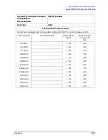
Page 169: ...ords Agilent Technologies Company Model 8753ES Serial Number Report Number Option s Date 2 External Source Mode Frequency Range Note If your analyzer does not have Option 006 write N A in all entries above 3 GHz Test Frequencies GHz Results 0 010 0 020 0 100 1 000 2 000 3 000 4 000 5 000 6 000 ...

Page 170: ... Power Level Accuracy Note If your analyzer does not have Option 006 write N A in all entries above 3 GHz Test Frequency Test Port Output Power dBm Specification dB Measured Value dBm Measurement uncertainty dB 300 kHz 0 1 0 47 20 MHz 0 1 0 14 50 MHz 0 1 0 14 100 MHz 0 1 0 14 200 MHz 0 1 0 14 500 MHz 0 1 0 14 1 GHz 0 1 0 13 2 GHz 0 1 0 13 3 GHz 0 1 0 27 4 GHz 0 1 0 17 5 GHz 0 1 0 17 6 GHz 0 1 0 17...

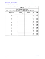
Page 171: ... Report Number Option s Date 4 Test Port Output Power Linearity Frequency Range 300 kHz to 3 GHz Power Setting dBm Marker 1 Maximum dB Marker 2 Minimum dB Specification dB Meas Uncert dB 15 0 2 0 04 13 0 2 0 03 11 0 2 0 03 9 0 2 0 03 7 0 2 0 03 5 0 2 0 03 3 0 2 0 02 1 0 2 0 02 1 0 2 0 02 3 0 2 0 02 5 0 2 0 03 7 0 5 0 03 8 0 5 0 03 9 0 5 0 03 10 0 5 0 03 ...

Page 172: ... 3 GHz to 6 GHz Note If your analyzer does not have Option 006 write N A in all entries above 3 GHz Power Setting dBm Marker 1 Maximum dB Marker 2 Minimum dB Specification dB Meas Uncert dB 15 0 2 0 04 13 0 2 0 03 11 0 2 0 03 9 0 2 0 03 7 0 2 0 03 5 0 2 0 03 3 0 2 0 02 1 0 2 0 02 1 0 2 0 02 3 0 2 0 02 5 0 2 0 03 7 0 5 0 03 8 0 5 0 03 9 0 5 0 03 10 0 5 0 03 ...

Page 173: ...el Level Note If your analyzer does not have Option 006 write N A in all entries above 3 GHz CW Frequency Specification dBm Test Port Power R Channel Power Measurement Uncertainty dB 300 kHz 35 1 0 3 29 MHz 35 1 0 3 31 MHz 35 1 0 15 90 MHz 35 1 0 16 10 MHz 35 1 0 30 90 MHz 35 1 0 31 10 MHz 35 1 0 1 6069 GHz 35 1 0 1 6071 GHz 35 1 0 3 000 GHz 35 1 0 4 000 GHz 30 2 0 5 000 GHz 30 2 0 6 000 GHz 30 2 ...

Page 174: ... A in all entries above 3 GHz Frequency Range Test Port IF Bandwidth Specification dBm a a Specifications in parentheses are valid for analyzers with Option 075 Calculated Value Meas Uncert dB 300 kHz 3 GHz Port 1 3 kHz 82 80 2 0 300 kHz 3 GHz Port 1 10 Hz 102 100 2 0 300 kHz 3 GHz Port 2 10 Hz 102 100 2 0 300 kHz 3 GHz Port 2 3 kHz 82 80 2 0 3 GHz 6 GHz Port 2 3 kHz 77 2 0 3 GHz 6 GHz Port 2 10 H...

Page 175: ...rial Number Report Number Option s Date 7 Test Port Input Frequency Response Note If your analyzer does not have Option 006 write N A in all entries above 3 GHz Frequency Range Test Port Specification dB Measured Value dB Meas Uncert dB 300 kHz 3 GHz Port 2 1 0 47 300 kHz 3 GHz Port 1 1 0 47 3 GHz 6 GHz Port 1 2 0 17 3 GHz 6 GHz Port 2 2 0 17 ...

Page 176: ...on s Date 8 Test Port Crosstalk Note If your analyzer does not have Option 006 write N A in all entries above 3 GHz Test Settings Specification dB Measured Value dB Measurement Uncertainty dB Crosstalk to Test Port 2 300 kHz 3 GHz 100 1 0 Crosstalk to Test Port 1 300 kHz 3 GHz 100 1 0 Crosstalk to Test Port 1 3 GHz 6 GHz 90 2 0 Crosstalk to Test Port 2 3 GHz 6 GHz 90 2 0 ...

Page 177: ...8 Directivity 3 GHz 6 GHz 25 0 8 Forward Direction Source Match 300 kHz 1 3 GHz 16 0 2 Source Match 1 3 GHz 3 GHz 16 0 2 Source Match 3 GHz 6 GHz 14 0 3 Reverse Direction Trans Tracking 300 kHz 1 3 GHz 1 0 0 006 Trans Tracking 1 3 GHz 3 GHz 1 0 0 009 Trans Tracking 3 GHz 6 GHz 1 5 0 021 Forward Direction Refl Tracking 300 kHz 1 3 GHz 1 0 0 001 Refl Tracking 1 3 GHz 3 GHz 1 0 0 005 Refl Tracking 3 ...

Page 178: ...B Measured Value dB Meas Uncert dB Reverse Direction Directivity 300 kHz 1 3 GHz 35 0 9 Directivity 1 3 GHz 3 GHz 30 0 8 Directivity 3 GHz 6 GHz 25 0 8 Reverse Direction Source Match 300 kHz 1 3 GHz 16 0 2 Source Match 1 3 GHz 3 GHz 16 0 2 Source Match 3 GHz 6 GHz 14 0 3 Reverse Direction Refl Tracking 300 kHz 1 3 GHz 1 0 0 001 Refl Tracking 1 3 GHz 3 GHz 1 0 0 005 Refl Tracking 3 GHz 6 GHz 1 5 0 ...

Page 179: ...6 rms A R 3 kHz Phase 0 038 rms A R 3 kHz Magnitude 0 006 dB rms B R 3 kHz Magnitude 0 006 dB rms B R 3 kHz Phase 0 038 rms B R 10 Hz Phase 0 006 rms B R 10 Hz Magnitude 0 001 dB rms Test Frequency 6 GHz Note If your analyzer does not have Option 006 write N A in all entries above 3 GHz A R 10 Hz Magnitude 0 002 dB rms A R 10 kHz Phase 0 012 rms A R 3 kHz Phase 0 070 rms A R 3 Hz Magnitude 0 010 d...

Page 180: ...Magnitude Dynamic Accuracy Test Port 2 G F G F Test Port Input Power dBm 8496A Attn dB Real Part Imag Part Test Port Measurement dB Expected Measurement Corrected dB Dynamic Accuracy Calculated Spec dB Meas Uncer dB 10 0 0 033 0 008 20 ref 10 0 000 0 021 0 008 30 20 0 031 0 008 40 30 0 041 0 008 50 40 0 054 0 008 60 50 0 069 0 017 70 60 0 111 0 017 80 70 0 257 0 017 90 80 0 741 0 017 100 90 2 121 ...

Page 181: ...gnitude Dynamic Accuracy Test Port 1 G F G F Test Port Input Power dBm 8496A Attn dB Real Part Imaginary Part Test Port Measurement dB Expected Measurement Corrected dB Dynamic Accuracy Calculated Spec dB Meas Uncer dB 10 0 0 033 0 008 20 ref 10 0 000 0 021 0 008 30 20 0 031 0 008 40 30 0 041 0 008 50 40 0 054 0 008 60 50 0 069 0 017 70 60 0 111 0 017 80 70 0 257 0 017 90 80 0 741 0 017 100 90 2 1...

Page 182: ...st Port Receiver Magnitude Compression Note If your analyzer does not have Option 006 write N A in all entries above 3 GHz Measured Value CW Frequency Test Port 2 Test Port 1 Specification dB Measurement Uncertainty dB 300 kHz 0 42 0 04 50 MHz 0 42 0 04 1 GHz 0 42 0 04 1 65 GHz 0 42 0 04 2 GHz 0 42 0 04 3 GHz 0 42 0 04 4 GHz 0 76 0 05 5 GHz 0 76 0 05 6 GHz 0 76 0 05 ...

Page 183: ...ort Number Option s Date 13 Test Port Receiver Phase Compression Note If your analyzer does not have Option 006 write N A in all entries above 3 GHz Measured Value CW Frequency Test Port 2 Test Port 1 Specification Measurement Uncertainty 300 kHz 6 0 3 50 MHz 6 0 3 1 GHz 6 0 3 1 65 GHz 6 0 3 2 GHz 6 0 3 3 GHz 6 0 3 4 GHz 7 2 0 4 5 GHz 7 2 0 4 6 GHz 7 2 0 4 ...

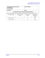
Page 184: ...8753ES Serial Number Report Number Option s Date 14 Test Port Output Input Harmonics Analyzers with Option 002 Test Description Specification dBc Measurement Value dBc Measurement Uncertainty dB Test Port Output Harmonics 2nd 25 1 5 3rd 25 1 5 Port 1 Input Harmonics 2nd 15 1 5 3rd 30 1 5 Port 2 Input Harmonics 2nd 15 1 5 3rd 30 1 5 ...

Page 185: ...in all entries above 3 GHz Analyzer Freq Fund Ext Source Freq Harm Power Meter Meas Cable Loss A Power Meter Cable Loss B Network Analyzer Reading A B Harm Meas Accy Spec dB Meas Uncert dB 20 MHz 40 MHz 1 5 0 17 20 MHz 60 MHz 1 5 0 17 100 MHz 200 MHz 1 5 0 17 100 MHz 300 MHz 1 5 0 17 300 MHz 600 MHz 1 5 0 17 300 MHz 900 MHz 1 5 0 17 500 MHz 1 GHz 1 5 0 17 500 MHz 1 5 GHz 1 5 0 17 1 GHz 2 GHz 1 5 0...

Page 186: ...2 160 Chapter2 System Verification and Performance Tests Agilent 8753ES Performance Test Records This page intentionally left blank ...

Page 187: ...n 006 6 GHz operation If your analyzer does not have Option 006 write N A for entries above 3 GHz Calibration Lab Address Report Number Date Last Calibration Date Customer s Name Performed by Model 8753ET Serial No Options Firmware Revision Ambient Temperature C Relative Humidity Test Equipment Used Description Model Number Trace Number Cal Due Date Frequency Counter Power Meter Power Sensor Calib...

Page 188: ... 300 003 0 000 000 520 5 0 4 999 950 5 000 050 0 000 008 610 16 0 15 999 840 16 000 160 0 000 028 220 31 0 30 999 690 31 000 310 0 000 053 730 60 999 999 60 999 389 61 000 609 0 000 104 800 121 0 120 998 790 121 001 210 0 000 206 800 180 0 179 998 200 180 001 800 0 000 307 200 310 0 309 996 900 310 003 100 0 000 528 300 700 0 699 993 000 700 007 000 0 001 191 700 1 300 0 1 299 987 1 300 013 0 002 ...

Page 189: ...ords Agilent Technologies Company Model 8753ET Serial Number Report Number Option s Date 2 External Source Mode Frequency Range Note If your analyzer does not have Option 006 write N A in all entries above 3 GHz Test Frequencies GHz Results 0 010 0 020 0 100 1 000 2 000 3 000 4 000 5 000 6 000 ...

Page 190: ... 3 GHz Test Frequency Minimum Valuea dBm a Values in parentheses pertain to analyzers with Option 004 Measured Value Maximum Valuea dBm Measurement Uncertainty dB 300 kHz 6 0 11 0 4 0 9 0 0 47 20 MHz 6 0 11 0 4 0 9 0 0 25 50 MHz 6 0 11 0 4 0 9 0 0 12 100 MHz 6 0 11 0 4 0 9 0 0 12 200 MHz 6 0 11 0 4 0 9 0 0 12 500 MHz 6 0 11 0 4 0 9 0 0 12 1 GHz 6 0 11 0 4 0 9 0 0 12 2 GHz 6 0 11 0 4 0 9 0 0 15 3 G...

Page 191: ... 4 Reflection Test Port Output Power Linearity for analyzers without Option 004 Frequency Range 300 kHz to 3 GHz Power Setting dBm PowerOffset dBm Marker 1 Maximum Marker 2 Minimum Spec dB Meas Uncert dB 20 15 0 5 0 04 18 13 0 5 0 03 16 11 0 5 0 03 14 9 0 2 0 03 12 7 0 2 0 03 10 5 0 2 0 03 8 3 0 2 0 02 6 1 0 2 0 02 4 1 0 2 0 02 2 3 0 2 0 02 0 5 0 5 0 03 3 8 0 5 0 03 5 10 0 5 0 03 ...

Page 192: ...d Frequency Range 3 GHz to 6 GHz Note If your analyzer does not have Option 006 write N A in all entries above 3 GHz Power Setting dBm PowerOffset dBm Marker 1 Maximum Marker 2 Minimum Spec dB Meas Uncert dB 20 15 0 5 0 04 18 13 0 5 0 03 16 11 0 5 0 03 14 9 0 2 0 03 12 7 0 2 0 03 10 5 0 2 0 03 8 3 0 2 0 02 6 1 0 2 0 02 4 1 0 2 0 02 2 3 0 2 0 02 0 5 0 5 0 03 3 8 0 5 0 03 5 10 0 5 0 03 ...

Page 193: ...Number Option s Date 5 Reflection Test Port Output Power Linearity for analyzers with Option 004 Frequency Range 300 kHz to 3 GHz Power Setting dBm Marker 1 Maximum Marker 2 Minimum Spec dB Meas Uncert dB 15 0 2 0 04 13 0 2 0 03 11 0 2 0 03 9 0 2 0 03 7 0 2 0 03 5 0 2 0 03 3 0 2 0 02 1 0 2 0 02 1 0 2 0 02 3 0 2 0 02 5 0 5 0 03 7 0 5 0 03 9 0 5 0 03 10 0 5 0 03 ...

Page 194: ...ption 004 continued Frequency Range 3 GHz to 6 GHz Note If your analyzer does not have Option 006 write N A for entries above 3 GHz Power Setting dBm Marker 1 Maximum Marker 2 Minimum Spec dB Meas Uncert dB 15 0 2 0 04 13 0 2 0 03 11 0 2 0 03 9 0 2 0 03 7 0 2 0 03 5 0 2 0 03 3 0 2 0 02 1 0 2 0 02 1 0 2 0 02 3 0 2 0 02 5 0 5 0 03 7 0 5 0 03 9 0 5 0 03 10 0 5 0 03 ...

Page 195: ... R Channel Level Note If your analyzer does not have Option 006 write N A in all entries above 3 GHz CW Frequency R Channel Power Specification dBm Measurement Uncertainty dB 300 kHz 35 1 5 3 29 MHz 35 1 5 3 31 MHz 35 1 5 15 90 MHz 35 1 5 16 10 MHz 35 1 5 30 90 MHz 35 1 5 31 10 MHz 35 1 5 1 6069 GHz 35 1 5 1 6071 GHz 35 1 5 3 000 GHz 30 1 5 4 000 GHz 30 1 5 5 000 GHz 30 1 5 6 000 GHz 30 1 5 ...

Page 196: ...ort Number 7 Transmission Test Port Input Noise Floor Level Note If your analyzer does not have Option 006 write N A for entries above 3 GHz Frequency Range IF Bandwidth Calculated Value Specification dBm Measurement Uncertainty dBm 300 kHz to 3 0 GHz 3 kHz 90 1 0 300 kHz to 3 0 GHz 10 Hz 110 1 0 3 GHz to 6 0 GHz 10 Hz 105 2 0 3 GHz to 6 0 GHz 3 kHz 85 2 0 ...

Page 197: ...Company Model 8753ET Serial Number Report Number Option s Date 8 Transmission Test Port Input Frequency Response Note If your analyzer does not have Option 006 write N A in all entries above 3 GHz Frequency Range Measured Value dB Specification dB Measurement Uncertainty dB 300 kHz to 3 GHz 1 0 47 3 GHz to 6 GHz 2 0 17 ...

Page 198: ...Technologies Company Model 8753ET Serial Number Report Number Option s Date 9 Test Port Crosstalk Note If your analyzer does not have Option 006 write N A in all entries above 3 GHz Frequency Range Measured Value dB Specification dB Measurement Uncertainty dB 300 kHz to 3 GHz 100 1 0 3 GHz to 6 GHz 90 2 0 ...

Page 199: ...GHz Test Description Frequency Range Spec dB Measured Value dB Meas Uncert dB Forward Direction Directivity 300 kHz to 1 3 GHz 30 0 9 Directivity 1 3 GHz to 3 GHz 24 0 6 Directivity 3 GHz to 6 GHz 19 0 8 Forward Direction Standard Source Match 300 kHz to 1 3 GHz 25 1 3 Source Match 1 3 GHz to 3 GHz 20 1 5 Source Match 3 GHz to 6 GHz 14 1 3 Forward Direction Option 004 Source Match 300 kHz to 1 3 G...

Page 200: ...s above 3 GHz Test Description Frequency Range Spec dB Measured Value dB Meas Uncert dB Forward Direction Refl Tracking 300 kHz to 1 3 GHz 1 0 0 009 Refl Tracking 1 3 GHz to 3 GHz 1 0 0 019 Refl Tracking 3 GHz to 6 GHz 2 0 0 030 Forward Direction Load Match 300 kHz to 1 3 GHz 24 0 2 Load Match 1 3 GHz to 3 GHz 19 0 2 Load Match 3 GHz to 6 GHz 16 0 2 Forward Direction Trans Tracking 300 kHz to 1 3 ...

Page 201: ...n 10 Hz Magnitude 0 001 dB rms Transmission 10 Hz Magnitude 0 001 dB rms Transmission 10 Hz Phase 0 006 rms Transmission 3 kHz Phase 0 038 rms Transmission 3 kHz Magnitude 0 006 dB rms Test Frequency 6 GHz Note If your analyzer does not have Option 006 write N A in all entries above 3 GHz Reflection 3 kHz Magnitude 0 010 dB rms Reflection 3 kHz Phase 0 070 rms Reflection 10 Hz Phase 0 012 rms Refl...

Page 202: ...2 176 Chapter2 System Verification and Performance Tests Agilent 8753ET Performance Test Records ...

Page 203: ...3 1 3 Adjustments and Correction Constants ...

Page 204: ...gnitude and Phase Correction Constants Test 53 on page 3 16 Cavity Oscillator Frequency Correction Constants Test 54 on page 3 26 Serial Number Correction Constants Test 55 on page 3 31 Option Numbers Correction Constants Test 56 on page 3 32 Initialize EEPROMs Test 58 on page 3 33 EEPROM Backup Disk Procedure on page 3 34 Correction Constants Retrieval Procedure on page 3 35 Loading Firmware on p...

Page 205: ...ce Pretune CC Test 48 RF Output Power CC Test 47 Sampler Magnitude and Phase CC Test 53 Cavity Oscillator Frequency CC Test 54 Source Spur Avoidance Tracking EEPROM Backup Disk Test Port Output Frequency Range and Accuracy Test Port Output Power Level Accuracy Test Port Output Power Linearity Test Port Output Input Harmonics Option 002 only A4 A5 A6 Samplers A9 Switch Positions Sampler Magnitude a...

Page 206: ...CC Test 53 IF Amplifier CC Test 51 EEPROM Backup Disk Test Port Input Noise Floor Level Test Port Crosstalk System Trace Noise A11 Phase Lock A9 Switch Positions Analog Bus CC Test 46 Pretune Default CC Test 45 Source Pretune CC Test 48 EEPROM Backup Disk Minimum R Channel Level Test Port Output Frequency Range and Accuracy A12 Reference A9 Switch Positions High Low Band Transition Frequency Accur...

Page 207: ...put Power Linearity Test Port Input Frequency Response Test Port Crosstalk Test Port Receiver Magnitude Compression Test Port Receiver Phase Compression Harmonic Measurement Accuracy Option 002 8753ES A22 Test Port Couplera A9 Switch Positions Sampler Magnitude and Phase CC Test 53 IF Amplifier CC Test 51 EEPROM Backup Disk Test Port Input Frequency Response Test Port Crosstalk Test Port Receiver ...

Page 208: ... the cover toward the rear of the instrument 6 Move the switch as shown in Figure 3 1 Move the A9 switch to the Alter position before you run any of the correction constant adjustment routines This is the position for altering the analyzer s correction constants Move the A9 switch to the Normal position after you have run correction constant adjustment routines This is the position for normal oper...

Page 209: ...nternal adjustment routine writes default correction constants for the source power accuracy 1 Press 2 Observe the analyzer for the results of the adjustment routine If the analyzer displays Source Def DONE you have completed this procedure If the analyzer displays Source Def FAIL refer to Chapter 7 Source Troubleshooting Preset System SERVICE MENU TESTS 44 x1 EXECUTE TEST YES ...

Page 210: ...inutes This adjustment writes default correction constants for rudimentary phase lock pretuning accuracy 1 Press 2 Observe the analyzer for the results of this adjustment routine If the analyzer displays Pretune Def DONE you have completed this procedure If the analyzer displays FAIL refer to Chapter 7 Source Troubleshooting Preset System SERVICE MENU TESTS 45 x1 EXECUTE TEST YES ...

Page 211: ...ng three reference voltages ground 0 37 and 2 5 volts then stores the calibration data as correction constants in EEPROMs 1 Press 2 Observe the analyzer for the results of the adjustment routine If the analyzer displays ABUS Cor DONE you have completed this procedure If the analyzer displays ABUS Cor FAIL refer to Chapter 6 Digital Control Troubleshooting Preset System SERVICE MENU TESTS 46 x1 EXE...

Page 212: ...minutes This procedure generates pretune values for correct phase locked loop operation 1 Press 2 Observe the analyzer for the results of this adjustment routine If the analyzer displays Pretune Cor DONE you have completed this procedure If the analyzer displays FAIL refer to Chapter 7 Source Troubleshooting Preset System SERVICE MENU TESTS 48 x1 EXECUTE TEST YES ...

Page 213: ...rve or change its GPIB address 4 Press to toggle between the 438A 437 and 436A power meters Choose the appropriate model number Use the 438A 437 selection if the power meter is an E4419B or E4418B NOTE If you are using the 438A power meter connect the 8482A power sensor to channel A and the 8481A power sensor to channel B Description HP Agilent Part or Model Number Power Meter 436A 437B 438A or E4...

Page 214: ...r If you make a mistake press and re enter the correct value d Press to complete the data entry for each point NOTE The following terms are part of the sensor calibration menu 8 For Option 006 Instruments Only Press to create a power sensor calibration table for power sensor B 8481A using the softkeys mentioned above 9 Connect the equipment as shown in Figure 3 2 allows you to select a frequency p...

Page 215: ...ructions at the prompts and press 13 When the analyzer completes the test observe the display for the results If you see DONE press and you have completed this procedure If you see FAIL re run this routine in the following order a Press b Repeat Source Default Correction Constants Test 44 on page 3 7 c Repeat RF Output Power Correction Constants Test 47 on page 3 11 System SERVICE MENU TESTS 47 x1...

Page 216: ...tine If DONE is displayed you have completed this procedure If FAIL is displayed check that the RF cable is connected between Port 1 and Port 2 Then repeat this adjustment routine If the analyzer continues to fail the adjustment routine refer to Chapter 6 Digital Control Troubleshooting Description HP Agilent Part Number Antistatic Wrist Strap 9300 1367 Antistatic Wrist Strap Cord 9300 0980 Static...

Page 217: ...y by shifting small signals to the most linear part of the ADC quantizing curve 1 Press NOTE This routine takes about three minutes 2 Observe the analyzer for the results of the adjustment routine If the analyzer displays ADC Ofs Cor DONE you have completed this procedure If the analyzer displays ADC Ofs Cor FAIL refer to Chapter 6 Digital Control Troubleshooting Preset System SERVICE MENU TESTS 5...

Page 218: ...l as required to observe or change its GPIB address 4 Press to toggle between the 438A 437 and 436A power meters Choose the appropriate model number Description HP Agilent Part or Model Number Power Meter 436A437B 438A or E4418B 4419B GPIB Cable 10833A Antistatic Wrist Strap 9300 1367 Antistatic Wrist Strap Cord 9300 0980 Static control Mat and Ground Wire 9300 0797 Additional Equipment for 50Ω An...

Page 219: ...alue d Press to complete the data entry for each point NOTE The following terms are part of the sensor calibration menu 7 For Option 006 Instruments Only Zero and calibrate the power meter and HP 8481A power sensor Then press to create a power sensor calibration table for power sensor B 8481A using the softkeys mentioned above 8 If you have an 8753ES go to Determine the Insertion Loss of the Cable...

Page 220: ... Figure 3 3 Figure 3 3 First Connections for Insertion Loss Measurement 8753ES 5 Press and then when the analyzer is done measuring the through 6 Press to save the calibration that you just made 7 Make the connections as shown in Figure 3 4 Figure 3 4 Second Connection for Insertion Loss Measurement Preset Meas Trans FWD S21 B R Center 1 G n Span 50 M µ Cal CAL KIT CAL KIT 7mm RETURN CALIBRATE MEN...

Page 221: ...rement 8753ET 4 Perform a 1 port calibration by performing the following steps a Press b Press c Connect the open from the calibration kit to the Reflection port as shown in Figure 3 5 d Press e Press f Connect the short to the Reflection port as shown in Figure 3 5 g Press h Remove the short from the Reflection port then connect the load to the Reflection port as shown in Figure 3 5 Press then Sc...

Page 222: ...Record this calculated value as the insertion loss of the cable It will be used later in this procedure Proceed to Sampler Correction Constants Routine next Sampler Correction Constants Routine 1 Press and answer at the prompt 2 The analyzer displays CONNECT 3 GHz SENSOR A TO PORT 1 8753ES or CONNECT 3 GHz SENSOR A TO REFL PORT 8753ET Make the connections as shown in Figure 3 7 using the 8482A pow...

Page 223: ...repeat the Sampler Correction Constants Routine on page 3 20 b The 8482A power sensor is connected to Port 1 Then repeat the Sampler Correction Constants Routine on page 3 20 4 For Option 006 Instruments Only When the analyzer displays CONNECT 6 GHz SENSOR B TO PORT 1 8753ES or CONNECT 6 GHz SENSOR B TO REFL PORT 8753ET make the connections as shown in Figure 3 7 using the 8481A power sensor Then ...

Page 224: ...For 8753ES only a Press This part of the test will take about 10 minutes b For Option 006 Instruments Only When the analyzer displays CONNECT 6 GHz SENSOR TO PORT 2 make the connections as shown in Figure 3 8 using the HP Agilent 8481A power sensor Then press This part of the test will take about 20 seconds 7 When the analyzer displays CONNECT PORT 1 TO PORT 2 connect the second through cable for ...

Page 225: ...he insertion loss of the through cable determined previously and press For example if the insertion loss of the through cable at 1 GHz was found to be 0 25 dB then press 11 When the analyzer completes the test observe the display for the results If you see Sampler Cor DONE you have completed this procedure If you see Sampler Cor FAIL it is necessary to adjust the sampler gain offset values which a...

Page 226: ...select the sampler to be tested or 4 Go to step 1 in Sampler Offset continued next Sampler Offset continued 1 Press 2 Press 3 Press 4 Read the marker s power value from the top of the display Be sure to retain the sign or of the value 5 Perform the following calculation using the following instructions Sampler Offset ROUND 4 0 4 0 marker value Subtract the marker value from 4 0 Multiply the result...

Page 227: ... new values 6 Go to Finish or to the next sampler to be adjusted R Channel Sampler 1 Access the first address by pressing 2 Enter the new value for the R sampler offset at the accessed address by pressing new value for R 3 Access the second address by pressing 4 Enter the new value at the accessed address by pressing 5 Press for the analyzer to use the new values 6 Go to Finish or to the next samp...

Page 228: ...be 10 dB to 20 dB 3 to 4 divisions above the trace noise Without the filter you need to distinguish the target spur between four or five spurs each of which may be 0 002 to 0 010 dB invisible to 2 divisions above or below the trace noise Perform the first five steps of the procedure at least once for familiarization before trying to select the target spur especially if you are not using a filter D...

Page 229: ...peatedly Watch the trace on each sweep and try to spot the target spur With the filter the target spur will be one of two obvious spurs see Figure 3 11 Without the filter not recommended the target spur will be one of four or five less distinct spurs as shown in Figure 3 12 and Figure 3 13 When the center frequency increases to 2994 999 MHz and you have not selected the target spur the message Cav...

Page 230: ...target spur will appear to the right of a second spur similar to Figure 3 11 6 Rotate the front panel knob to position the marker on the spur and then press 7 Observe the analyzer for the results of this adjustment routine If the analyzer displays Cav Osc Cor DONE you have completed this procedure If the analyzer does not display DONE repeat this procedure If the analyzer continues not to display ...

Page 231: ...imes as necessary to thoroughly inspect the current span The target spur usually appears as one of a group of four evenly spaced spurs as in Figure 3 12 The target spur is the right most spur fourth from the left On any particular sweep one any or all of the spurs may be large small visible invisible above or below the reference line Figure 3 12 Typical Display of Four Spurs without a Filter On oc...

Page 232: ...pattern some up some down and the target spur itself almost indistinguishable Figure 3 14 Target Spur Is Almost Invisible 10 Rotate the front panel knob to position the marker on the target spur Then press and observe the analyzer for the results of the adjustment routine If the analyzer displays Cav Osc Cor DONE you have completed this procedure If the analyzer displays FAIL refer to Chapter 7 So...

Page 233: ...correct mistakes after you perform step 5 unless you contact the factory for a clear serial number keyword Then you must perform the Option Numbers Correction Constants Test 56 on page 3 32 and repeat this procedure 5 Press 6 Observe the analyzer for the results of the routine If the analyzer displays the message Serial Cor DONE you have completed this procedure If the analyzer does not display DO...

Page 234: ...nal keyboard or by rotating the front panel knob to position the arrow below each character of the keyword and then pressing to enter each letter Press if you made a mistake 4 Press when you have finished entering the title CAUTION Do not confuse I with 1 one or O with 0 zero 5 Press 6 Observe the analyzer for the results of the adjustment routine If the analyzer displays Option Cor DONE you have ...

Page 235: ...zer disk drive and press b Use the front panel knob to highlight the filename that represents your serial number c Press If you don t have the correction constants backed up on a disk run all the internal service routines in the following order Source Default Correction Constants Test 44 Source Pretune Correction Constants Test 45 Analog Bus Correction Constants Test 46 ADC Offset Correction Const...

Page 236: ...lay The file type ISTATE E indicates that the file is an instrument state with EEPROM backup 4 Press Use the front panel knob and the softkey or an external keyboard to rename the file FILE0 TO N12345 where 12345 represents the last 5 digits of the instrument s serial number The first character in the filename must be a letter When you are finished renaming the file press 5 Write the following inf...

Page 237: ...5 where N12345 represents the file name of the EEPROM data for the analyzer On the factory shipped EEPROM backup disk the filename is FILE1 4 Press to download the correction constants data into the instrument EEPROMs 5 Press and verify that good data was transferred to EEPROM by performing a simple measurement 6 Move the A9 switch back to the Normal position when you are done working with the ins...

Page 238: ...nt state and press 3 Press 4 If the instrument state file was not saved to disk with the same name that it had while in internal memory you may wish to rename the file Press enter the desired name and press 5 Repeat steps 1 through 4 for each instrument state that you wish to save 6 Turn off the network analyzer 7 Insert the firmware disk into the instrument s disk drive 8 Turn the instrument on T...

Page 239: ...acceptable firmware filename was not found on the disk The desired format for firmware filenames is 8753Ex_7 _yz where x either S or T and where yz the latest firmware revision number Check that the firmware disk used was for the 8753ET ES If any of the following LED patterns are present the firmware disk may be defective If any other LED pattern is present the CPU board is defective LED Pattern C...

Page 240: ...ll be blank during this time At the end of a successful loading the LEDs for Channel 1 and Port 1 on an 8753ES will remain on and the display will turn on indicating the version of firmware that was loaded In Case of Difficulty If the firmware did not load successfully LED patterns on the front panel can help you isolate the problem If the following LED pattern is present an acceptable firmware fi...

Page 241: ...firmware disk may be defective If any other LED pattern is present the CPU board is defective NOTE If firmware did not load a red LED on the CPU board will be flashing If the following LED pattern is present on the CPU board suspect the disk drive or associated cabling LED Pattern CH1 CH2 R L T S O O O front of instrument ...

Page 242: ...1 marker is as many divisions above the reference line as the channel 2 marker is below it See Figure 3 16 8 To fine tune this adjustment press to set FRAC N TUNE to 29 2 MHz Description HP Agilent Part Number Non metallic adjustment tool 8830 0024 Antistatic wrist strap 9300 1367 Antistatic wrist strap cord 9300 0980 Static control table mat and ground wire 9300 0797 Preset Display DUAL QUAD SETU...

Page 243: ...ants Fractional N Frequency Range Adjustment Figure 3 15 Location of the FN VCO TUNE Adjustment Figure 3 16 Fractional N Frequency Range Adjustment Display 9 Press Meas ANALOG IN Aux Input 29 x1 Marker Format MORE REAL Scale Ref REFERENCE VALUE 7 x1 ...

Page 244: ...ent If the marker value is less than 7 you have completed this procedure If the marker value is greater than 7 readjust FN VCO ADJ to 7 Then perform steps 2 to 10 to confirm that the channel 1 and channel 2 markers are still above and below the reference line respectively If you cannot adjust the analyzer correctly replace the A14 board assembly ...

Page 245: ...e the upper rear bumpers and analyzer top cover 2 Connect the equipment as shown in Figure 3 17 Description HP Agilent Part or Model Number Spectrum analyzer 8563E RF Cable 50Ω Type N 24 inch 8120 4781 Non metallic adjustment tool 8830 0024 Antistatic wrist strap 9300 1367 Antistatic wrist strap cord 9300 0980 Static control table mat and ground wire 9300 0797 Additional Equipment for 50Ω Analyzer...

Page 246: ...d 3 For Option 1D5 Instruments Only Remove the BNC to BNC jumper that is connected between the EXT REF and the 10 MHz Precision Reference as shown in Figure 3 19 4 Set the spectrum analyzer measurement parameters as follows or for Option 006 or for Option 006 5 On the network analyzer press or for Option 006 FREQUENCY 3 G n 6 G n Span 60 kHz 120 kHz AMPLITUDE REF LEVEL LL 10 dBm Preset Sweep Setup...

Page 247: ...surement within specifications 7 Replace the A12 assembly if you are unable to adjust the frequency as specified Repeat this adjustment test Figure 3 18 Location of the VCXO ADJ Adjustment NOTE To increase the accuracy of this adjustment the following steps are recommended 8 Replace the instrument covers and wait 15 minutes in order to allow the analyzer to reach its precise operating temperature ...

Page 248: ...igh Stability Frequency Adjustment Location 11 Insert a narrow screwdriver and adjust the high stability frequency reference potentiometer for a CW frequency measurement within specification In Case of Difficulty Replace the A26 assembly if you cannot adjust the CW frequency within specification ...

Page 249: ...ent is necessary follow these steps a Adjust the VCO tune see Figure 3 21 to position the left half of the trace to 0 125 mV The variable capacitor C85 has a half turn tuning range if the A12 Reference Board is part number 08753 60209 and seven turns if the part number is 08753 60357 Be careful not to overtighten and damage the seven turn capacitor b Adjust the HBLB see Figure 3 21 to position the...

Page 250: ...3 48 Chapter3 Adjustments and Correction Constants High Low Band Transition Adjustment Figure 3 20 High Low Band Transition Adjustment Trace Figure 3 21 High Low Band Adjustment Locations ...

Page 251: ...ipment as shown in Figure 3 22 2 Make sure the instruments are set to their default GPIB addresses 8753ES ET 16 spectrum analyzer 18 Description HP Agilent Part or Model Number Spectrum analyzer 8563E GPIB Cable 10833A B C D RF Cable 50Ω Type N 24 inch 8120 4781 Cable 50Ω Coax BNC m to BNC m 10503A Non metallic adjustment tool 8830 0024 Antistatic wrist strap 9300 1367 Antistatic wrist strap cord ...

Page 252: ...ure 3 22 Fractional N Spur Avoidance and FM Sideband Adjustment Setup 3 Set the spectrum analyzer measurement parameters as follows Reference Level 0 dBm Resolution Bandwidth 100 Hz Center Frequency 676 145105 MHz Span 2 5 kHz 4 On the analyzer press Preset Avg IF BW 3000 x1 Sweep Setup CW FREQ 676 045105 M µ ...

Page 253: ...7515 MHz 10 On the analyzer press 11 Adjust the API2 R43 for a null minimum amplitude on the spectrum analyzer 12 On the spectrum analyzer set the center frequency for 676 003450 MHz 13 On the analyzer press 14 Adjust the API3 R45 for a null minimum amplitude on the spectrum analyzer 15 On the spectrum analyzer set the center frequency for 676 003045 MHz 16 On the analyzer press 17 Adjust the API4...

Page 254: ...C center conductor alligator clip to A11 TP10 labeled φ ERR the shield clip to A11 TP1 GND as shown in Figure 3 24 Figure 3 24 Location of A11 Test Points and A3 CAV ADJ Adjustments 2 Press 3 Press 4 Press 5 To make sure that you have connected the test points properly adjust the CAV ADJ potentiometer while observing the analyzer display You should notice a change in voltage Description HP Agilent...

Page 255: ...s are not visible on the analyzer display see Figure 3 25 no adjustment is necessary If spikes are excessive see Figure 3 25 adjust the CAV ADJ potentiometer see Figure 3 24 on the A3 source bias assembly to eliminate the spikes If the spikes persist refer to Chapter 7 Source Troubleshooting Figure 3 25 Display of Acceptable versus Excessive Spikes ...

Page 256: ... after an entry enables the option Pressing after an entry disables the option 5 Repeat steps 3 and 4 for all of the unprotected options that you want to enable 6 After you have entered all of the instrument s hardware options press the following keys 7 View the analyzer display for the listed options 8 When you have entered all of the hardware options return the A9 switch to the Normal position 9...

Page 257: ...lect and if you want to load the files for the Fractional N Frequency Range Adjustment How to Set Up the Fractional N Frequency Range Adjustment 1 Remove the right rear bumpers and right side cover This exposes the adjustment location in the sheet metal 2 Press where X is the sequence number 3 Adjust the FN VCO TUNE with a non metallic tool so that the channel 1 marker is as many divisions above t...

Page 258: ...just the HBLB A12 R68 to position the right half of the trace 125 to 175 mV about 1 to 1 5 divisions higher than the left half Refer to Chapter 7 Source Troubleshooting if you cannot perform the adjustment How to Set Up the Fractional N Spur Avoidance and FM Sideband Adjustment 1 Press where X is the sequence number 2 Remove the upper rear corner bumpers and the top cover using a TORX screwdriver ...

Page 259: ...POINTS 11 x1 COUPLED CHAN OFF START 36 M u STOP 60 75 M u SWEEP SETUP SWEEP TIME 12 5 k m MEAS ANALOG IN 29 x1 FN VCO TUN SCALE REF 0 6 x1 REF VALUE 7 x1 MKR CH 2 SWEEP SETUP CW FREQ 31 0001 M u SWEEP TIME 12 375 k m MEAS ANALOG IN 29 x1 FN VCO TUN SCALE REF 2 x1 REF VALUE 6 77 x1 MKR 6 k m Sequence FNCHK checks the VCO adjustment SWEEP SETUP CW FREQ 1 G n SYSTEM SERVICE MENU ANALOG BUS ON SERVICE...

Page 260: ...spur adjustments TITLE SP 2 5K PERIPHERAL HPIB ADDR 18 x1 TITLE TO PERIPHERAL WAIT x 0 x1 TITLE AT 0DB TITLE TO PERIPHERAL WAIT x 0 x1 TITLE RB 100HZ TITLE TO PERIPHERAL WAIT x 0 x1 TITLE CF 676 145105MZ TITLE TO PERIPHERAL WAIT x 0 x1 CW FREQ 676 045105M u TITLE ADJ A13 100KHZ SEQUENCE PAUSE TITLE CF 676 051105MZ TITLE TO PERIPHERAL WAIT x 0 x1 CW FREQ 676 048105M u TITLE ADJ A13 API1 SEQUENCE PA...

Page 261: ... 007515MZ TITLE TO PERIPHERAL WAIT x 0 x1 CW FREQ 676 004515M u TITLE ADJ A13 API2 SEQUENCE PAUSE TITLE CF 676 003450MZ TITLE TO PERIPHERAL WAIT x 0 x1 CW FREQ 676 000450M u TITLE ADJ A13 API3 SEQUENCE PAUSE TITLE CF 676 003045MZ TITLE TO PERIPHERAL WAIT x 0 x1 CW FREQ 676 000045M u TITLE ADJ A13 API4 ...

Page 262: ...3 60 Chapter3 Adjustments and Correction Constants Sequences for Mechanical Adjustments ...

Page 263: ...4 1 4 Start Troubleshooting Here ...

Page 264: ... fault Locate the specific troubleshooting procedures to identify the assembly or peripheral at fault To identify the portion of the analyzer at fault follow these procedures Step 1 Initial Observations on page 4 5 Step 2 Operator s Check on page 4 6 Step 3 GPIB Systems Check on page 4 8 Step 4 Faulty Group Isolation on page 4 10 ...

Page 265: ...th the appropriate troubleshooting chapter that identifies the faulty assembly 2 Order a replacement assembly Refer to Chapter 13 Replaceable Parts 3 Replace the faulty assembly and determine what adjustments are necessary Refer to Chapter 14 Assembly Replacement and Post Repair Procedures 4 Perform the necessary adjustments Refer to Chapter 3 Adjustments and Correction Constants 5 Perform the nec...

Page 266: ...gies sales or service office to determine the warranty on your instrument and whether repair will be on site or return to Agilent Technologies 1 Choose the nearest Agilent Technologies service center Refer to Table 15 1 on page 15 3 2 Include a detailed description of any failed test and any error message 3 Ship the analyzer using the original or comparable antistatic packaging materials ...

Page 267: ...zer Self Test 1 Disconnect all devices and peripherals from the analyzer 2 Switch on the analyzer and press 3 Watch for the indications shown in Figure 4 1 to determine if the analyzer is operating correctly Figure 4 1 Preset Sequence If the self test failed refer to Step 4 Faulty Group Isolation on page 4 10 Preset ...

Page 268: ...nsfer switch An S11 measurement is stored in memory and the switch is toggled to Port 2 and then back to Port 1 where another S11 measurement is made The difference between the memory trace and the second trace is switch repeatability This procedure is absent from the routine for the 8753ET since it lacks a transfer switch The remaining part of the test exercises the internal attenuator in 10 dB s...

Page 269: ...T 22 Port 2 Op Chk in the active entry area 9 Repeat steps 4 through 7 For an 8753ET You will be prompted to connect a cable between the Reflection and Transmission ports 10 If both tests pass the analyzer is about 80 verified If either test fails refer to Step 4 Faulty Group Isolation on page 4 10 or a Make sure that the connection is tight Repeat the test b Visually inspect the connector interfa...

Page 270: ...ddress set on each device must match the one recognized by the analyzer and displayed Peripheral addresses are often set with a rear panel switch Refer to the manual of the peripheral to read or change its address If Using a Plotter or Printer 1 Ensure that the plotter or printer is set up correctly Power is on Pens and paper loaded Pinch wheels are down Some plotters need to have P1 and P2 positi...

Page 271: ...shooting Systems with Controllers on page 4 9 or Step 4 Faulty Group Isolation on page 4 10 If the resultant trace does not start at 1 MHz suspect the GPIB function of the analyzer refer to Chapter 6 Digital Control Troubleshooting Troubleshooting Systems with Multiple Peripherals Connect any other system peripherals but not a controller to the analyzer one at a time and check their functionality ...

Page 272: ...aulty The four functional groups are power supplies digital control source receiver Descriptions of these groups are provided in Chapter 12 Theory of Operation The checks in the following pages must be performed in the order presented If one of the procedures fails it is an indication that the problem is in the functional group checked Go to the troubleshooting information for the indicated group ...

Page 273: ...er See Figure 4 3 The upper red LED should be off The lower green LED should be on Figure 4 3 A15 Preregulator LEDs Check the A8 Post Regulator LEDs Remove the analyzer s top cover Switch on the power Inspect the green LEDs along the top edge of the A8 post regulator assembly All green LEDs should be on The fan should be audible In case of difficulty refer to Chapter 5 Power Supply Troubleshooting...

Page 274: ... off after a few seconds except the Chan 1 LED 8753ES Only the Port 2 LED goes off and the Port 1 LED illuminates See Figure 4 4 The display should come up bright with no irregularity in colors After an initial pattern five red LEDs on the A9 CPU board should remain off They can be observed through a small opening in the rear panel If the power up sequence does not occur as described or if there a...

Page 275: ...l test and possibly others have failed the analyzer reports the first failure detected Refer to Chapter 6 Digital Control Troubleshooting If the analyzer indicates failure but does not identify the test press to search for the failed test Then refer to Chapter 6 Digital Control Troubleshooting Likewise if the response to front panel or GPIB commands is unexpected troubleshoot the digital control g...

Page 276: ...ne stage but phase lock could not be acquired thereafter PHASE LOCK LOST Phase lock was acquired but then lost PHASE LOCK CAL FAILED An internal phase lock calibration routine is automatically executed at power on when pretune values drift or when phase lock problems are detected A problem spoiled a calibration attempt POSSIBLE FALSE LOCK The analyzer is achieving phase lock but possibly on the wr...

Page 277: ...er should remain approximately 0 dBm throughout the analyzer frequency range Repeat this step at 1 and 3 GHz For Option 006 include an additional check at 6 GHz If any incorrect power levels are measured refer to Chapter 7 Source Troubleshooting No Oscilloscope or Power Meter Try the ABUS 1 Monitor ABUS node 16 by pressing 2 Press 3 The display should resemble Figure 4 6 Preset Sweep Setup CW FREQ...

Page 278: ...Chapter4 Start Troubleshooting Here Source Figure 4 6 ABUS Node 16 1 V GHz If any of the above procedures provide unexpected results or if error messages are present refer to Chapter 7 Source Troubleshooting ...

Page 279: ...number 8120 4779 for 50Ω analyzers and 8120 2408 for 75Ω analyzers Figure 4 7 Equipment Setup 2 Press 3 Observe the measurement trace displayed by the A input The trace should have about the same flatness as the trace in Figure 4 8 4 Press 5 Observe the measurement trace displayed by the B input The trace should have about the same flatness as the trace in Figure 4 8 Preset Meas INPUT PORTS A TEST...

Page 280: ...OWER REDUCED CAUTION OVERLOAD ON INPUT R POWER REDUCED The error messages above indicate that you have exceeded approximately 14 dBm at one of the test ports The RF output power is automatically reduced to 85 dBm The annotation P appears in the left margin of the display to indicate that the power trip function has been activated When this occurs press and enter a lower power level Press to switch...

Page 281: ...s as the trace in Figure 4 9 B Input 1 Disconnect the short from the Reflection port and connect the through cable between the Reflection and Transmission ports 2 Press 3 Observe the measurement trace displayed by the B input The trace should have about the same flatness as the trace in Figure 4 10 Description HP Agilent Part or Model Number Short Part of 85032B Calibration Kit Cable 50Ω Type N 81...

Page 282: ...4 20 Chapter4 Start Troubleshooting Here Receiver 8753ET Figure 4 9 A Input Typical Measurement Trace Figure 4 10 B Input Typical Measurement Trace ...

Page 283: ...ON INPUT R POWER REDUCED The error messages above indicate that you have exceeded approximately 14 dBm at one of the test ports The RF output power is automatically reduced to 20 dBm or 85 dBm for Option 004 The annotation P appears in the left margin of the display to indicate that the power trip function has been activated When this occurs press and enter a lower power level Press to switch on t...

Page 284: ...ct cables calibration or verification kit devices limiters and adapters can all induce system problems Reconfigure the system as it is normally used and reconfirm the problem Continue with Chapter 9 Accessories Troubleshooting Accessories Error Messages POWER PROBE SHUT DOWN The biasing supplies to a front panel powered device like a probe or millimeter module are shut down due to excessive curren...

Page 285: ...ion 014 and is intended to be used as a guide in finding and fixing problems with the 8753ES Option 014 only For information on troubleshooting the standard instrument refer to the appropriate sections of this service guide The Option 014 troubleshooting guide is divided into sections called Symptoms Each symptom corresponds to a possible problem experienced during the operation of the analyzer in...

Page 286: ...mper Configuration In this configuration all of the standard self tests and performance tests are the same as the standard 8753ES Required Equipment and Tools Figure 4 12 Standard Mode Jumper Configuration Description HP Agilent Part or Model Number TORX T 10 Screwdriver Torque Wrench 5 16 incha a The torque is 8 inch pounds 8710 1765 Calibration Kit 7mm 85031B RF Cable APC 7 24 inch 610mm 8120 47...

Page 287: ...If a problem occurs match the measurement S11 S21 S12 S22 where the problem was displayed to the symptom that closest describes the problem For information on how to make measurements refer to your analyzer s user s guide 1 Measure the S21 response by pressing 2 Measure the S12 response by pressing 3 Disconnect the cable from PORT 2 4 Connect a short to the end of the test port cable 5 Measure the...

Page 288: ...5 Example of Frequency Roll Off are examples of what an irregular or a degraded signal might look like These plots are intended to be used only as examples for troubleshooting Symptoms one through four include sample plots of what irregular or degraded signals may look like for the different S parameter measurements described in the symptom CAUTION If problems are experienced and replacement parts...

Page 289: ...Chapter 4 4 27 Start Troubleshooting Here Troubleshooting 8753ES Option 014 Figure 4 14 Example of a Power Hole Figure 4 15 Example of Frequency Roll Off ...

Page 290: ...e can be found on the jumper take a look at the SWITCH and COUPLER ports on the front panel Inspect for damage to the ports Look for damage to the center conductor bent pin or damaged threads on either port Replace any damaged ports 2 If no problems are found during inspection of the ports reconnect the jumper from PORT 1 SWITCH port to the PORT 1 COUPLER port Make sure that the jumper is connecte...

Page 291: ...OUPLER ports on the front panel Inspect for damage to the ports Look for damage to the center conductor bent pin or damaged threads on either port Replace any damaged ports 2 If no problems are found during inspection of the ports reconnect the jumper between the PORT 1 A IN and the PORT 1 A OUT port Make sure that the jumper is connected correctly Improper connections will cause power holes in th...

Page 292: ...PLER ports on the front panel Inspect for damage to the ports Look for damage to the center conductor bent pin or damaged threads on either port Replace any damaged ports 2 If no problems are found during inspection of the ports reconnect the jumper between the PORT 2 SWITCH and the PORT 2 COUPLER port Make sure that the jumper is connected correctly Improper connections will cause power holes in ...

Page 293: ...OUPLER ports on the front panel Inspect for damage to the ports Look for damage to the center conductor bent pin or damaged threads on either port Replace any damaged ports 2 If no problems are found during inspection of the ports reconnect the jumper between the PORT 2 B IN and the PORT 2 B OUT port Make sure that the jumper is connected correctly Improper connections will cause power holes in th...

Page 294: ...t panel Inspect for damage to the ports Look for damage to the center conductor bent pin or damaged threads on either port Replace any damaged ports 2 If no problems are found during inspection of the ports reconnect the jumper between the RF IN and the RF OUT port Make sure that the jumper is connected correctly Improper connections will cause power holes in the frequency response 3 If the proble...

Page 295: ...URCE MP1 S S S S S S 1st IF 1MHz 1MHz 1MHz 1st LO 1st LO 1st LO 4kHz 4kHz 4kHz A6P 1 6 A5P 1 6 2nd IF A4P 1 6 2nd LO 2nd LO 2nd LO L ON H 15MHz TO 2 99GHz STD H 15MHz TO 5 99 OPT 006 L ON H 15MHz TO 2 99GHz STD H 15MHz TO 5 99 OPT 006 L ON H 15MHz TO 2 99GHz STD H 15MHz TO 5 99 OPT 006 L 0 014 TO 16 004MHz H 996kHz L 0 014 TO 16 004MHz H 996kHz L 0 014 TO 16 004MHz H 996kHz L 10kHz TO 16 00MHz H 1...

Page 296: ...O 2 99GHz STD H 15MHz TO 5 99 OPT 006 L ON H 15MHz TO 2 99GHz STD H 15MHz TO 5 99 OPT 006 L ON H 15MHz TO 2 99GHz STD H 15MHz TO 5 99 OPT 006 L 0 014 TO 16 004MHz H 996kHz L 0 014 TO 16 004MHz H 996kHz L 0 014 TO 16 004MHz H 996kHz L 10kHz TO 16 00MHz H 1 000MHz L 10kHz TO 16 00MHz H 1 000MHz L 10kHz TO 16 00MHz H 1 000MHz 10kHz TO 3GHz STD 10kHz TO 6GHz OPT 006 10kHz TO 3GHz STD 10kHz TO 6GHz OPT...

Page 297: ...5 1 5 Power Supply Troubleshooting ...

Page 298: ...ow the procedures in the order given unless an error message appears on the display refer to Error Messages on page 5 17 the fan is not working refer to Fan Troubleshooting on page 5 19 The power supply group assemblies consist of the following A8 post regulator A15 preregulator All assemblies however are related to the power supply group because power is supplied to each assembly ...

Page 299: ...p with the appropriate troubleshooting chapter that identifies the faulty assembly 2 Order a replacement assembly Refer to Chapter 13 Replaceable Parts 3 Replace the faulty assembly and determine what adjustments are necessary Refer to Chapter 14 Assembly Replacement and Post Repair Procedures 4 Perform the necessary adjustments Refer to Chapter 3 Adjustments and Correction Constants 5 Perform the...

Page 300: ...k Diagram Figure 5 1 shows the power supply group in simplified block diagram form Refer to the detailed block diagram of the power supply located at the end of this chapter to see voltage lines and specific connector pin numbers Figure 5 1 Power Supply Group Simplified Block Diagram ...

Page 301: ...teadily on page 5 7 If the red LED is on or flashing refer to If the Red LED of the A15 Is ON on page 5 8 Figure 5 2 Location of A15 Diagnostic LEDs Check the Green LEDs on A8 Remove the top cover of the analyzer and locate the A8 post regulator use the location diagram under the top cover if necessary Check to see if the green LEDs on the top edge of A8 are all on There are nine green LEDs one is...

Page 302: ...locations and Table 5 3 for supply voltages and limits Figure 5 3 A8 Post Regulator Test Point Locations Table 5 1 A8 Post Regulator Test Point Voltages TP Supply Range 1 65 V not used 64 6 to 65 4 2 AGND n a 3 5 VD 4 9 to 5 3 4 SDIS n a 5 15 V 14 4 to 15 6 6 12 6 VPP probe power 12 1 to 12 91 7 15 V 14 5 to 15 5 8 5 VU 5 05 to 5 35 9 5 2 V 5 0 to 5 4 10 22 V 21 3 to 22 7 11 6 V 5 8 to 6 2 ...

Page 303: ...or switch setting and actual line voltage to see that they are all correct Figure 5 4 shows how to remove the line fuse using a small flat blade screwdriver to pry out the fuse holder Figure 5 2 shows the location of the line voltage selector switch Use a small flat blade screwdriver to select the correct switch position NOTE Refer to 8753ET ES Hardware Preregulator on page 13 55 for the correct l...

Page 304: ...ch on the analyzer and observe the red LED on A15 If the red LED goes out the problem is probably the A8 post regulator Continue to Verify the A15 Preregulator on page 5 10 to first verify that the inputs to A8 are correct If the red LED is still on fuse F4 in the preregulator A15 may need to be replaced if the line voltage selector switch was set to 120 V and the instrument was connected to a 220...

Page 305: ...Chapter 5 5 9 Power Supply Troubleshooting If the Red LED of the A15 Is ON Figure 5 5 Power Supply Cable Locations ...

Page 306: ...ce A15 is verified Continue to Check for a Faulty Assembly on page 5 11 Table 5 2 Output Voltages Pin A15W1P1 Disconnected Voltages A8J2 Connected Voltages A15 Preregulator Label 1 N C 68 to 76 2 N C 2 125 to 100 68 to 76 2 70 V 3 4 22 4 to 33 6 17 0 to 18 4 18 V 5 6 22 4 to 33 6 17 0 to 18 4 18 V 7 N C 7 4 to 8 0 N C 8 9 4 to 14 7 4 to 8 0 8 V 9 10 9 4 to 14 6 7 to 7 4 8 V 11 N C 24 6 to 28 6 N C...

Page 307: ... A8 Refer to Figure 5 5 3 Remove or disconnect the assemblies listed in Table 5 3 one at a time and in the order shown The assemblies are sorted from most to least accessible Table 5 3 also lists any associated assemblies that are supplied by the assembly that is being removed After each assembly is removed or disconnected switch on the analyzer and observe the red LED on A15 CAUTION Always switch...

Page 308: ...lty Inspect the Motherboard If the red LED is still on after replacement or repair of A15 switch off the analyzer and inspect the motherboard for solder bridges and other noticeable defects Use an ohmmeter to check for shorts The 5 VD 5 VCPU or 5 VDSENSE lines may be bad Refer to the block diagram at the end of this chapter and troubleshoot these suspected power supply lines on the A17 motherboard...

Page 309: ...eadily except for the 5 VD LED the A15 preregulator and A8 post regulator are working properly and the trouble is excessive loading somewhere after the motherboard connections at A8 Continue to Remove the Assemblies on page 5 13 Check the A8 Fuses and Voltages Check the fuses along the top edge of A8 If any A8 fuse has burned out replace it If it burns out again when power is applied to the analyz...

Page 310: ...r after each assembly is installed The assembly that causes the green LEDs to go off or flash could be faulty NOTE It is possible however that this condition is caused by the A8 post regulator not supplying enough current To check this reinstall the assemblies in a different order to change the loading If the same assembly appears to be faulty replace that assembly If a different assembly appears ...

Page 311: ...zer 6 Of those assemblies that are left on the list remove or disconnect them from the analyzer one at a time Table 5 4 shows the best order in which to remove them sorting them from most to least accessible Table 5 4 also lists any associated assemblies that are supplied by the assembly that is being removed After each assembly is removed or disconnected switch on the analyzer and observe the LED...

Page 312: ...bly to Remove Removal or Disconnection Method Other Assemblies that Receive Power from the Removed Assembly 1 A3 Source Remove from Card Cage None 2 A7 Pulse Generator Remove from Card Cage None 3 A4 R Sampler Remove from Card Cage None 4 A5 A Sampler Remove from Card Cage None 5 A6 B Sampler Remove from Card Cage None 6 A9 CPU Disconnect W35 and W36 A20 Disk Drive 7 A2 Front Panel Interface Disco...

Page 313: ...gulated power supplies on A8 have been shut down Check the temperature of the operating environment it should not be greater than 55 C 131 F The fan should be operating and there should be at least 15 cm 6 in spacing behind and all around the analyzer to allow for proper ventilation PROBE POWER SHUT DOWN The front panel RF probe biasing supplies are shut down due to excessive current draw These su...

Page 314: ...with each of these supplies near the A8 test points If these fuses keep burning out a short exists Try isolating A8 by removing it from the motherboard connector but keeping the cable A15W1 connected to A8J2 Connect a jumper wire from A8TP2 to chassis ground If either the 15 V or 12 6 V fuse blows or the associated green LEDs do not light replace A8 If the 15 V and 12 6 V green LEDs light troubles...

Page 315: ...of the A8P1 connector The 18 V supply is regulated on A8 but changes the voltage to the fan depending on airflow and temperature information Its voltage ranges from approximately 1 0 volts to 14 7 volts and connects to the A17 motherboard via pin 31 of the A8P1 connector Measure the voltages of these supplies while using an extender board to allow access to the PC board connector A8P1 Short A8TP3 ...

Page 316: ...oblems Preset states that appear spontaneously without pressing typically signal a power supply or A9 CPU problem Since the A9 CPU assembly is the easiest to substitute do so If the problem ceases replace the A9 If the problem continues replace the A15 preregulator assembly Preset ...

Page 317: ......

Page 318: ...6 1 6 Digital Control Troubleshooting ...

Page 319: ... Start Troubleshooting Here The digital control group assemblies consist of the following CPU A9 Display A2 A18 A19 A27 Front Panel A1 A2 Digital IF A10 Rear Panel Interface A16 Begin with CPU Troubleshooting A9 on page 6 5 then proceed to the assembly that you suspect has a problem If you suspect an GPIB interface problem refer to GPIB Failures on page 6 19 ...

Page 320: ...Chapter 6 6 3 Digital Control Troubleshooting Digital Control Group Block Diagram Digital Control Group Block Diagram Figure 6 1 Digital Control Group Block Diagram ...

Page 321: ...up with the appropriate troubleshooting chapter that identifies the faulty assembly 2 Order a replacement assembly Refer to Chapter 13 Replaceable Parts 3 Replace the faulty assembly and determine what adjustments are necessary Refer to Chapter 14 Assembly Replacement and Post Repair Procedures 4 Perform the necessary adjustments Refer to Chapter 3 Adjustments and Correction Constants 5 Perform th...

Page 322: ...NORMAL position do the following 1 Remove the power line cord from the analyzer 2 Set the analyzer on its side 3 Remove the two corner bumpers from the bottom of the instrument with a T 15 TORX screwdriver 4 Loosen the captive screw on the bottom cover s back edge 5 Slide the cover toward the rear of the instrument 6 Move the switch to the NORMAL position as shown in Figure 6 2 7 Replace the botto...

Page 323: ...eed to the assembly that you suspect has a problem If the LEDs did not remain off switch off the power and remove the bottom cover for further troubleshooting Figure 6 3 CPU LED Window on Rear Panel 2 Cycle the power while observing all eight red LEDs With the analyzer positioned bottom up cycle the power and observe the eight red LEDs while looking from the front of the instrument NOTE If firmwar...

Page 324: ...s Dark Stuck Pixels Newtons Rings Evaluate the display as follows If either the A18 LCD A19 GSP A9 CPU or A27 backlight inverter assemblies are replaced perform a visual inspection of the display If it appears that there is a problem with the display refer to the troubleshooting information that follows If the new display appears dim or doesn t light see Backlight Intensity Check next Backlight In...

Page 325: ...nutes of warmup time Zero the photometer according to the manufacturer s instructions 4 Center the photometer on the analyzer display as shown in Figure 6 4 Figure 6 4 Backlight Intensity Check Setup NOTE The intensity levels are read with a display bezel installed 5 If the photometer registers less than 50 Nits the display backlight lamp is bad Refer to the Chapter 14 Assembly Replacement and Pos...

Page 326: ...ifications Dark stuck on pixels may appear against a white background To test for these dots press In a properly working display the following will not occur more than 12 stuck pixels not to exceed a maximum of 7 red green or blue more than one occurrence of 2 consecutive stuck pixels stuck pixels less than 6 5 mm apart Newton s Rings To check for the patterns known as Newton s Rings change the di...

Page 327: ...ge on the external monitor is normal then suspect A2 A18 or the front panel cabling If the image on the external monitor is bad suspect the A19 GSP or cable W20 CPU to motherboard Troubleshooting a Black Display 1 Remove the front panel with the exception of leaving cable W17 A2 to motherboard connected 2 Press while checking to see if there is a flash of light If the light does not flash suspect ...

Page 328: ...on page 10 14 Confirm that there are four intensities for each color If the test passes then continue If the test fails then suspect the front panel cabling A2 A19 or A18 3 Connect a VGA monitor to the analyzer If the image on the external monitor has the same color problems then replace the A19 GSP If the image on the external monitor is acceptable then there must be a missing color bit Suspect t...

Page 329: ... If all the front panel LEDs either stay on or off there is a control problem between A9 and A1 A2 See Inspect Cables on page 6 15 If at the end of the turn on sequence the Chan 1 LED is not on and all GPIB status LEDs are not off continue with Identify the Stuck Key on page 6 13 If you suspect that one or more LEDs have burned out replace the A1 keypad assembly NOTE Port 1 and Port 2 LED problems...

Page 330: ...k key Free the stuck key or replace the front panel part causing the problem The Chan 3 and Chan 4 LEDs are not used LED is on The footswitch is an accessory that can be set up through a rear panel port Table 6 1 Front Panel Key Codes Decimal Number LED Pattern Key Chan 1 Chan 2 R L T S 0 1 2 3 4 5 6 7 8 9 10 11 12 13 14 15 16 Footswitch 17 18 19 20 21 G n 9 M µ 6 k m 3 x1 8 7 5 4 2 1 0 Local Syst...

Page 331: ...ed 32 33 34 35 36 37 38 39 Not Used 40 41 42 43 44 45 46 47 Table 6 1 Front Panel Key Codes Decimal Number LED Pattern Key Chan 1 Chan 2 R L T S Save Recall Copy Entry Off Scale Ref Cal Marker Fctn Power Sweep Setup Chan 2 Chan 4 Format Avg Marker Search Stop Span Chan 1 Chan 3 Meas Display Marker Start Center Return ...

Page 332: ...e the cables are properly connected Replace any bad cables Test Using a Controller If a controller is available write a simple command to the analyzer If the analyzer successfully executes the command the problem is either the A2 front panel interface or W17 A2 to motherboard ribbon cable is faulty 48 49 50 51 52 53 54 55 Table 6 1 Front Panel Key Codes Decimal Number LED Pattern Key Chan 1 Chan 2...

Page 333: ...be run as part of one or both major test sequences all internal test 0 and preset test 1 1 Press to perform all INT tests 2 Then press to see the results of the preset test If either sequence fails press the keys to find the first occurrence of a FAIL message for tests 2 through 20 See Table 6 2 for further troubleshooting information System SERVICE MENU TESTS 0 x1 EXECUTE TEST 1 x1 ...

Page 334: ...A9 A10 Most likely A9 assembly 10 DIF Counter P AI A10 A9 A12 Check analog bus node 17 for 1 MHz If correct A12 is verified suspect A10 11 DSP Control P AI A10 A9 Most likely A10 12 Fr Pan Wr Rd A2 A1 A9 Run test 23 If fail replace A2 If pass problem is on bus between A9 and A2 or on A9 assembly 13 Rear Panel AI A16 A9 Disconnect A16 and check A9J2 pin 48 for 4 MHz clock signal If OK replace A16 I...

Page 335: ... the failure is intermittent do the following 1 Press to turn on the repeat function 2 Then press 3 Select the test desired and press 4 Press any key to stop the function The test repeat function is explained in Chapter 10 Service Key Menus and Error Messages System SERVICE MENU TEST OPTIONS REPEAT ON RETURN TESTS EXECUTE TEST ...

Page 336: ...s not check the GPIB paths external to the instrument Press If the analyzer fails the test the problem is likely to be the A16 rear panel If the analyzer passes the test it indicates that the A9 CPU can communicate with the A16 rear panel with a 50 confidence level There is a good chance that the A16 rear panel is working This is because internal bus lines have been tested between the A9 CPU and A...

Page 337: ...6 20 Chapter6 Digital Control Troubleshooting GPIB Failures ...

Page 338: ...7 1 7 Source Troubleshooting ...

Page 339: ...two troubleshooting procedures for the following problems Incorrect power levels Perform the Power troubleshooting checks on page 7 5 Phase lock error Perform the Phase Lock Error troubleshooting checks on page 7 6 The source group assemblies consist of the following A3 source A4 sampler mixer A7 pulse generator A11 phase lock A12 reference A13 fractional N analog A14 fractional N digital ...

Page 340: ...ith the appropriate troubleshooting chapter that identifies the faulty assembly 2 Order a replacement assembly Refer to Chapter 13 Replaceable Parts 3 Replace the faulty assembly and determine what adjustments are necessary Refer to Chapter 14 Assembly Replacement and Post Repair Procedures 4 Perform the necessary adjustments Refer to Chapter 3 Adjustments and Correction Constants 5 Perform the ne...

Page 341: ...efore You Start Troubleshooting Before You Start Troubleshooting Make sure all of the assemblies are firmly seated Also make sure that input R has a signal of at least 35 dBm about 0 01 Vp p into 50 ohms at all times to maintain phase lock ...

Page 342: ...ce the source 2 RF Output Power Correction Constants Test 47 Follow the instructions for this procedure given in RF Output Power Correction Constants Test 47 on page 3 11 The procedure is complete when DONE appears on the analyzer display Use a power meter to verify that power levels are now correct If power levels are not correct or if the analyzer fails the routine proceed with step 3 next 3 Sam...

Page 343: ...ned in the Source Group Troubleshooting Appendix on page 7 30 and should be used to troubleshoot phase lock problems The equipment setup shown in Figure 7 1 can be used throughout this chapter Phase Lock Loop Error Message Check Phase lock error messages may appear as a result of incorrect pretune correction constants To check this possibility perform the pretune correction constants routine The f...

Page 344: ...ce the bottom cover corner bumpers and power cord Figure 7 2 Switch Positions on the A9 CPU 2 Switch on the analyzer and press to generate new analog bus correction constants Then press to generate default pretune correction constants Press to generate new pretune correction constants 3 Press and observe the analyzer display No error message set the A9 CC switch to the NORMAL position Then refer t...

Page 345: ...nection Diagram 5 If the analyzer is an 8753ES and you connected W8 to A5 press A6 press 6 If the analyzer is an 8753ET and you connected W8 to A5 press A6 connect a cable between the Reflection and Transmission test ports and press 7 Ignore the displayed trace but check for phase lock error messages If the phase lock problem persists the R channel sampler is not the problem A3 Source and A11 Phas...

Page 346: ...ont panel knob or front panel keys to set the pretune frequency to 300 kHz 30 MHz and 40 MHz Verify the signal frequency on the oscilloscope NOTE In SRC TUNE mode the source output frequency changes in 1 to 2 MHz increments and should be 1 to 6 MHz above the indicated output frequency 4 Check for the frequencies indicated by Table 7 1 5 The signal observed on an oscilloscope should be as solid as ...

Page 347: ...e observed on the oscilloscope by a factor of ten 8 Note the results of the frequency and power changes If the frequency and power output changes are correct skip ahead to A12 Reference Check on page 7 12 If the frequency changes are not correct continue with YO Coil Drive Check with Analog Bus on page 7 11 If the power output changes are not correct check analog bus node 3 by performing the follo...

Page 348: ...z at Analog Bus Node 16 with Source PLL Off YO Coil Drive Check with Oscilloscope NOTE Use the large extender board for easy access to the voltage points The extender board is included with the 8753 Tool Kit See Chapter 13 Replaceable Parts for part numbers and ordering information 1 Connect oscilloscope probes to A11P1 1 and A11P1 2 The YO coil drive signal is actually two signals whose voltage d...

Page 349: ...ncy reference signals is to use the analog bus while referring to Table 7 2 Alternatively you can use an oscilloscope while referring to Table 7 3 and Figure 7 8 through Figure 7 14 If any of the observed signals differs from the figures there is a 90 probability that the A12 assembly is faulty Either consider the A12 assembly defective or perform the A12 Digital Control Signals Check on page 7 18...

Page 350: ...he counter readings match the frequencies listed in Table 7 2 skip ahead to A13 A14 Fractional N Check on page 7 20 If the counter readings are incorrect at the 500 kHz and 2 MHz settings only go to FN LO at A12 Check on page 7 16 If all the counter readings are incorrect at all three CW frequencies the counter may be faulty Perform the Oscilloscope Method check of the signals described next If th...

Page 351: ...nd typically 1 5 V in amplitude You may have to increase the oscilloscope intensity to see these pulses See Figure 7 8 Figure 7 8 Sharp 100 kHz Pulses at A13TP5 any frequency Table 7 3 A12 Reference Frequencies Mnemonic Signal Description Location See Figure Analyzer Setting FN100kHzREF 100 kHz Reference A13TP5 Figure 7 8 any REF Phase Lock Reference A11TP9 Figure 7 9 16 MHz CW REF Phase Lock Refe...

Page 352: ...7 10 High Band REF Signal In high band the REF signal is a constant 1 MHz square wave as indicated by Figure 7 9 Figure 7 9 High Band REF Signal 16 MHz CW Low Band REF Signal In low band this signal follows the frequency of the RF output signal Figure 7 10 illustrates a 5 MHz CW signal Figure 7 10 REF Signal at A11TP9 5 MHz CW If REF looks good skip ahead to 4 MHz Reference Signal on page 7 16 If ...

Page 353: ... to 60 8 MHz If the FN LO signal is good the A12 assembly is faulty If the FN LO signal is not good skip ahead to A13 A14 Fractional N Check on page 7 20 Figure 7 11 Typical FN LO Waveform at A12J1 4 MHz Reference Signal This reference signal is used to control the receiver If faulty this signal can cause apparent source problems because the CPU uses receiver data to control the source At A12TP9 i...

Page 354: ...out of phase Figure 7 13 90 Degree Phase Offset of High Band 2nd LO Signals 16 MHz CW In Phase 2nd LO Signals in Low Band The 2nd LO signals in low band as shown in Figure 7 14 are not phase shifted In low band these signals track the RF output with a 4 kHz offset Figure 7 14 In Phase Low Band 2nd LO Signals 14 MHz CW If any of the signals of Table 7 2 are incorrect the probability is 90 that the ...

Page 355: ...ger on the negative edge In preset state the signal should show activity similar to Figure 7 15 Figure 7 15 L ENREF Line at A12P2 16 Preset L HB and L LB Lines These complementary signals toggle when the instrument switches from low band to high band as illustrated by Figure 7 16 Table 7 4 A12 Related Digital Control Signals Mnemonic Signal Description Location See Figure Analyzer Setting L ENREF ...

Page 356: ...Chapter 7 7 19 Source Troubleshooting Phase Lock Error Figure 7 16 Complementary L HB and L LB Signals Preset If all of the digital signals appear good the A12 assembly is faulty ...

Page 357: ...oscope described next If the readings fail the specified limits perform the A14 VCO Exercise on page 7 22 A14 VCO Range Check with Oscilloscope 1 Remove the W9 HI OUT cable A14J1 to A7 from the A7 assembly and connect it to an oscilloscope set for 50 ohm input impedance Switch on the analyzer 2 Press to activate the FRACN TUNE service mode See Chapter 10 Service Key Menus and Error Messages for mo...

Page 358: ...Chapter 7 7 21 Source Troubleshooting Phase Lock Error Figure 7 17 10 MHz HI OUT Waveform from A14J1 Figure 7 18 25 MHz HI OUT Waveform from A14J1 ...

Page 359: ...itutes a power supply for the A13 assembly to check the frequency range of the A14 VCO 1 Switch off the analyzer and remove the A13 assembly 2 Put the A14 assembly on an extender board and switch on the instrument 3 Prepare to monitor the VCO frequency either by Activating the analog bus and setting the internal counter to the FRACN node or Connecting an oscilloscope to A14J2 labeled LO OUT and lo...

Page 360: ...de to avoid relock transitions and activate the FRACN TUNE service mode 3 Connect an oscilloscope to A14J3 and observe the output 4 With the FRACN TUNE service feature vary the frequency from 30 MHz to 60 8 MHz 5 The period of the observed signal should vary from 5 5 µs to 11 µs If this procedure produces unexpected results the A14 assembly is faulty If this procedure produces the expected results...

Page 361: ...hows relative inactivity of this signal during preset condition The lower trace shows its status during a 16 MHz to 31 MHz sweep with inactivity during retrace only Table 7 6 A14 to A13 Digital Control Signal Locations Mnemonic A13 Location A14 Location CST none TP3 L FNHOLD P2 2 P2 2 FNBIAS P2 5 P2 5 API1 P2 32 P2 32 API2 P2 3 P2 3 API3 P2 34 P2 34 API4 P2 4 P2 4 API5 P2 35 P2 35 FN LATCH P1 28 P...

Page 362: ...ulse generator assembly Set the analyzer to generate a 16 MHz CW signal Connect the spectrum analyzer to the A7 output connector and observe the signal The A7 comb should resemble the spectral display in Figure 7 23 Figure 7 23 Pulse Generator Output 2 If the analyzer malfunction relates to a particular frequency or range look more closely at the comb tooth there Adjust the spectrum analyzer span ...

Page 363: ...ll attached to the A14 assembly Narrow the span and bandwidth to observe the signal closely 5 If the HI OUT signal is as clean as Figure 7 25 the A7 assembly is faulty Otherwise check the A14 to A7 cable or recheck the A13 A14 fractional N as described ahead Rechecking the A13 A14 Fractional N Some phase lock problems may result from phase noise problems in the fractional N loop To troubleshoot th...

Page 364: ...yzer and tune the source to 50 MHz Press 4 Set the SRC TUNE frequency to those listed in Table 7 7 and observe the 1st IF waveforms They should appear similar to Figure 7 26 If the signals observed are proper continue with A11 Phase Lock Check on page 7 28 If the signals observed are questionable use a spectrum analyzer to perform the A7 Pulse Generator Check with Spectrum Analyzer on page 7 25 Ta...

Page 365: ...y operating mode with phase lock problems replace the A11 phase lock assembly Phase Lock Check with PLL DIAG Refer to Phase Lock Diagnostic Tools on page 7 30 for an explanation of the error messages and the diagnostic routines Follow the steps there to determine in which state the phase lock is lost If NO IF FOUND is displayed confirm that the analog bus is functional and perform Source Pretune C...

Page 366: ... block diagram in Chapter 4 as an aid to troubleshooting the problem to its source 5 If any of the output signals is not proper the A11 assembly is faulty Table 7 8 A11 Input Signals Mnemonic I O Access See Figure Notes FM COIL O A11P1 3 33 Figure 7 27 Aids YO COIL in setting YIG Press to observe this signal REF I A11TP9 Figure 7 9 Figure 7 10 Observe both low band and high band CW frequencies YO ...

Page 367: ...etune values was not successful a source or receiver failure Perform Source Pretune Correction Constants Test 48 on page 3 10 If the analyzer fails that routine perform the A4 Sampler Mixer Check on page 7 8 PHASE LOCK LOST means that phase lock was lost or interrupted before the band sweep ended a source problem Refer to Phase Lock Diagnostic Routines next to access the phase lock loop diagnostic...

Page 368: ... procedures in this chapter to check source functions at specific frequencies Broadband Power Problems This section assumes that a power problem exists across the full frequency range but that no error message is displayed on the analyzer The problem may affect Port 1 Port 2 or both Assemblies in question include A3 source A21 directional coupler A22 directional coupler 8753ES only A24 solid state...

Page 369: ...7 32 Chapter7 Source Troubleshooting Source Group Troubleshooting Appendix ...

Page 370: ...8 1 8 Receiver Troubleshooting ...

Page 371: ...roubleshooting Use this procedure only if you have read Chapter 4 Start Troubleshooting Here Follow the procedures in the order given unless instructed otherwise The receiver group assemblies consist of the following A4 A5 A6 sampler mixer assemblies A10 digital IF assembly ...

Page 372: ...with the appropriate troubleshooting chapter that identifies the faulty assembly 2 Order a replacement assembly Refer to Chapter 13 Replaceable Parts 3 Replace the faulty assembly and determine what adjustments are necessary Refer to Chapter 14 Assembly Replacement and Post Repair Procedures 4 Perform the necessary adjustments Refer to Chapter 3 Adjustments and Correction Constants 5 Perform the n...

Page 373: ...alyzer has exceeded approximately 14 dBm at one of the test ports The RF output power is automatically reduced to 85 dBm The annotation P appears in the left margin of the display to indicate that the power trip function has been activated To reset the analyzer s power and regain control of the power level do the following 1 Remove any devices under test which may have contributed excess power to ...

Page 374: ... MHz signal and substituting the A10 assembly or checking the signals listed in Table 8 1 on page 8 7 Check 2nd LO Check the 2nd LO signal Refer to A12 Reference Check on page 7 12 for analog bus and oscilloscope checks of the 2nd LO and waveform illustrations If the analyzer passes the checks continue to Check the 4 MHz REF Signal next If the analyzer fails the checks perform the High Low Band Tr...

Page 375: ... the 4 MHz reference signal at A10P2 6 If the signal does not resemble Figure 8 1 troubleshoot the signal source A12P2 36 and path If the signal is good the probability is greater than 90 that the A10 assembly is faulty For confirmation perform Check A10 by Substitution or Signal Examination next Figure 8 1 4 MHz REF Waveform Preset ...

Page 376: ... page 8 9 Otherwise troubleshoot the suspect signals or consider the A10 assembly faulty Table 8 1 Signals Required for A10 Assembly Operation Mnemonic Description A10 Location Signal Source See Figure DIFD0 Digital IF data 0 LSB P2 27 A9P2 27 DIFD1 Digital IF data 1 P2 57 A9P2 57 DIFD2 Digital IF data 2 P2 28 A9P2 28 DIFD3 Digital IF data 3 P2 58 A9P2 58 DIFD4 Digital IF data 4 P2 29 A9P2 29 DIFD...

Page 377: ...8 8 Chapter8 Receiver Troubleshooting Check the 4 MHz REF Signal Figure 8 2 Digital Data Lines Observed Using L INTCOP as Trigger Figure 8 3 Digital Control Lines Observed Using L INTCOP as Trigger ...

Page 378: ...check the 4 kHz output of the sampler mixer in question at the A10 assembly The input and output access pins are listed in Table 8 2 The signal should resemble the waveform of Figure 8 4 If the signal is good continue with Check the Trace with the Sampler Correction Constants Off on page 8 10 If the signal is bad skip ahead to Check 1st LO Signal at Sampler Mixer on page 8 10 Figure 8 4 2nd IF 4 k...

Page 379: ...ent when the sampler correction constants are toggled from off to on perform Sampler Magnitude and Phase Correction Constants Test 53 on page 3 16 If the trace remains bad after this adjustment the A10 assembly is defective Figure 8 5 Typical Trace with Sampler Correction On and Off Check 1st LO Signal at Sampler Mixer If the 4 kHz signal is bad at the sampler mixer assembly check the 1st LO signa...

Page 380: ...loscope checks of the 2nd LO and waveform illustrations Table 8 3 identifies the signal location at the samplers and the A12 assembly If the 2nd LO is good at the sampler mixer the sampler mixer assembly is faulty Otherwise troubleshoot the A12 assembly and associated signal path Table 8 3 2nd LO Locations Mnemonic Description Sampler Location Signal Source 2nd LO 1 2nd LO 0 degrees A4 5 6 P1 11 A...

Page 381: ...8 12 Chapter8 Receiver Troubleshooting Troubleshooting When One or More Inputs Look Good ...

Page 382: ...9 1 9 Accessories Troubleshooting ...

Page 383: ...n t affect the normal functioning of the analyzer but render incorrect measurement data Failures which impede the normal functioning of the analyzer or prohibit the use of a feature This chapter addresses the first category of failures which are usually caused by the following operator errors faulty calibration devices or connectors bad cables or adapters improper calibration techniques These fail...

Page 384: ... with the appropriate troubleshooting chapter that identifies the faulty assembly 2 Order a replacement assembly Refer to Chapter 13 Replaceable Parts 3 Replace the faulty assembly and determine what adjustments are necessary Refer to Chapter 14 Assembly Replacement and Post Repair Procedures 4 Perform the necessary adjustments Refer to Chapter 3 Adjustments and Correction Constants 5 Perform the ...

Page 385: ...ts of the test port center conductors and loose connector bulkheads 2 Inspect the calibration kit devices for bent or broken center conductors and other physical damage Refer to the calibration kit operating and service manual for information on gaging and inspecting the device connectors If any calibration device is obviously damaged or out of mechanical tolerance replace the device ...

Page 386: ...the same load on the other test port and measure its directivity If the second port looks bad as if the problem had shifted with the load replace the load If the second port looks good as if the load had not been the problem troubleshoot the first port Loads for 8753ET If the directivity error term looks good the load and the test port are good If directivity looks bad connect a known good load to...

Page 387: ...nd sex as the short and open in question If the devices are not from one of the standard calibration kits refer to your analyzer s user s guide for information on how to use the function Set aside the short and open that are causing the problem 1 Perform an S11 1 port calibration using the good short and open Then press to view the devices in Smith chart format 2 Connect the good short to port 1 P...

Page 388: ...oting Inspect the Error Terms Replace the good open with the questionable open at port 1 The trace of the questionable open should appear very similar to the known good open Figure 9 2 Typical Smith Chart Traces of Good Short a and Open b ...

Page 389: ...9 8 Chapter9 Accessories Troubleshooting Inspect the Error Terms ...

Page 390: ...10 1 10 Service Key Menus and Error Messages ...

Page 391: ...t control troubleshoot The main section of this chapter Service Key Menus divides the menus into three groups Internal Diagnostics Menus on page 10 3 Service Feature Menus on page 10 16 Firmware Revision Softkey on page 10 41 Additionally there are sections providing information on the following GPIB Service Mnemonic Definitions on page 10 42 Error Messages on page 10 44 ...

Page 392: ... Figure 10 1 and described in the following tables The following keys access the internal diagnostics menus Figure 10 1 Internal Diagnostics Menus NOTE Throughout this service guide these conventions are observed are labeled front panel keys are display defined keys in the menus GPIB COMMANDS when applicable TESTS TEST OPTIONS SELF DIAGNOSE Hardkeys SOFTKEYS ...

Page 393: ...65 Test Patterns 66 80 To access the first test in each category press the category softkey To access the other tests use the numeric keypad step keys or front panel knob The test number name and status abbreviation will be displayed in the active entry area of the display Table 10 1 shows the test status abbreviation that appears on the display its definition and the equivalent GPIB code The GPIB...

Page 394: ...rnal connections or user interaction N A Evaluate the analyzer s external operation These additional tests require some user interaction such as keystrokes N A Verifies the analyzer system operation by examining the contents of the measurement calibration arrays Refer to Chapter 2 System Verification and Performance Tests Information about the calibration arrays is provided in Chapter 11 Error Ter...

Page 395: ... tighter limits for the operator s check The SPCL limits are useful for a guard band PWRLOSS Selects whether or not to use the power loss table for a power meter calibration N A Accesses the power loss sensor lists menu that contains the following softkeys USESENS A B selects the A or B power sensor calibration factor list for use in power meter calibration measurements CALFSENA accesses the Edit ...

Page 396: ...uency point to be edited deleted from or added to the current data table Works with the entry controls SEDI D Allows modification of frequency cal factor and loss values previously entered in the current data table SDEL Deletes frequency cal factor and loss values previously entered in the current data table SADD Adds new frequency cal factor and loss values to the current data table up to a maxim...

Page 397: ...ests 2 3 and 4 then tests 5 11 14 15 and 16 If any of these tests fail this test returns a FAIL status Use the front panel knob to scroll through the tests and see which failed If all pass this test displays a PASS status Each test in the subset retains its own test status This same subset is available over GPIB as TST It is not performed upon remote preset 2 ROM Part of the ROM RAM tests and cann...

Page 398: ...front panel interface and processors A9 CPU data buffering and address decoding See also tests 23 and 24 This runs only when selected 13 GPIB Tests the ability of the A9 CPU main processor to write read to the rear panel control elements It tests the A16 rear panel and A9 CPU data buffering and address decoding It does not test the GPIB interface for that see the analyzer s programmer s guide This...

Page 399: ...0 to pass Table 10 6 External Tests Test Number Test Name Description 21 Port 1 Op Chk Part of Step 2 Operator s Check on page 4 6 The procedure requires the external connection of a short to PORT 1 22 Port 2 Op Chk Same as 21 but tests PORT 2 for 8753ES A through cable is required for the 8753ET 23 Fr Pan Seq Tests the front panel knob entry and all A1 front panel keys as well as the front panel ...

Page 400: ...te for system verification from an 8753ET ES verification disk in preparation for a measurement calibration It must be done before service internal tests 28 29 30 or 31 are performed 28 Ver Dev 1 Recalls verification limits from disk for verification device 1 in all applicable measurements It performs pass fail limit testing of the current measurement 29 Ver Dev 2 Same as 28 above for device 2 30 ...

Page 401: ... routine 51 IF Step Cor Measures the gain of the IF amplifiers A and B only located on the A10 digital IF to determine the correction constants for absolute amplitude accuracy It provides smooth dynamic accuracy and absolute amplitude accuracy in the 30 dBm input power region 52 ADC Ofs Cor Measures the A10 Digital IF ADC linearity characteristics using an internal ramp generator and stores values...

Page 402: ...0 DRAM cell Tests the DRAM on A19 by writing a test pattern to the DRAM and then verifying that it can be read back 61 Main VRAM Tests the VRAM by writing all zeros to one location in each bank and then writing all ones to one location in each bank Finally a walking one pattern is written to one location in each bank 62 VRAM bank Tests all the cells in each of the 4 VRAM banks 63 VRAM video Verifi...

Page 403: ...ern is also very useful when using an oscilloscope for troubleshooting The staircase pattern it produces will quickly show missing or stuck data bits 72 Test Pat 7 Displays the following seven colors Red Yellow Green Cyan Blue Magenta and White 73 Test Pat 8 This pattern is intended for use with an external display The pattern displays a color rainbow pattern for showing the ability of the A19 GSP...

Page 404: ...instead of one staircase between each horizontal sync pulse This pattern is used to troubleshoot the pixel processing circuit of the A19 GSP board 78 Test Pat 13 Displays a convergence pattern for measuring the accuracy of the color convergence of the external monitor 79 80 Test Pat 14 15 Displays crosshatch and inverse crosshatch patterns for testing color convergence linearization alignment This...

Page 405: ...2 and described in the following tables The following keys access the service feature menus Figure 10 2 Service Feature Menus Service Modes Menu The service modes menu allows you to control and monitor various circuits for troubleshooting To access this menu press SERVICE MODES ANALOG BUS on OFF PEEK POKE FIRMWARE REVISION System SERVICE MENU ...

Page 406: ...bleshooting N A Accesses the functions that allow you to adjust the source tests the pretune functions of the phase lock and source assemblies Use the entry controls to set test port output to any frequency from 300 kHz to 6 GHz When in this mode Set analyzer to CW frequency before pressing Test port output is 1 to 6 MHz above indicated entered frequency Instrument does not attempt to phase lock R...

Page 407: ...sed with the analog bus counter N A Used only with PLL DIAG mode indicates that it will continuously cycle through all steps of the phase lock sequence holds it at any step of interest This mode is useful for troubleshooting phase locked loop problems N A Provides access to the rest of the service modes keys SM5 Toggles the sampler correction routine ON for normal operation or OFF for diagnosis or...

Page 408: ...perating variations due to hardware limitations refer to Chapter 3 Adjustments and Correction Constants Having this information on disk is useful as a backup in case the constants are lost due to a CPU board failure Without a disk backup the correction constants can be regenerated manually although the procedures are more time consuming SM8 Offsets the frequency of both the A3 YIG oscillator and t...

Page 409: ...n can be the following the main ADC the frequency counter When analog bus traces are displayed frequency is the x axis For a linear x axis in time switch to CW time mode or sweep a single band The Main ADC The main ADC is located on the A10 digital IF assembly and makes voltage measurements in two ranges See Analog In Menu on page 10 21 for more information The Frequency Counter The frequency coun...

Page 410: ...Keys Key GPIB Mnemonic Description N A Allows you to monitor the analog bus nodes except nodes 1 2 3 4 9 10 12 with external equipment oscilloscope voltmeter etc To do this connect the equipment to the AUX INPUT BNC connector on the rear panel and press until is highlighted CAUTION To prevent damage to the analyzer first connect the signal to the rear panel AUX INPUT and then switch the function O...

Page 411: ...ower sweep on the analog bus Then follow the node specific instructions Step A3 Press N A Switches the counter to monitor the A14 fractional N VCO frequency at the node shown on the Overall Block Diagram in Chapter 4 Start Troubleshooting Here N A Switches the counter to monitor the A14 fractional N VCO frequency after it has been divided down to 100 kHz for phase locking the VCO Table 10 12 Analo...

Page 412: ...the analog bus Then press Node 1 is the output of the main power DAC It sets the reference voltage to the ALC loop At normal operation this node should read approximately 4 volts at 0 dBm with a slope of about 150 mV dB This corresponds to approximately 4 volts from 15 to 10 dBm Figure 10 3 Analog Bus Node 1 Meas ANALOG IN 1 x1 Scale Ref AUTO SCALE ...

Page 413: ...Hz Press the following to view analog bus node 2 Node 2 measures the voltage on the internal voltage controlled oscillator Or in normal operation it should read 1 V GHz Figure 10 4 Analog Bus Node 2 Preset Start 30 k m System SERVICE MENU ANALOG BUS ON Meas ANALOG IN 2 x1 Format MORE REAL Scale Ref AUTO SCALE ...

Page 414: ...analog node 3 Node 3 measures the current that goes to the main IF amplifier At normal operation this node should read about 15 mA from 30 kHz to 299 kHz 130 mA from 300 kHz to 3 GHz 500 mA from 3 GHz to 6 GHz Figure 10 5 Analog Bus Node 3 Preset System SERVICE MENU ANALOG BUS ON Meas ANALOG IN 3 x1 Format MORE REAL Scale Ref AUTO SCALE ...

Page 415: ...nentially follows the power level inversely Flat segments indicate ALC saturation and should not occur between 85 dBm and 10 dBm Figure 10 6 Analog Bus Node 4 Node 5 Temp temperature sensor This node registers the temperature of the cavity oscillator which must be known for effective spur avoidance The sensitivity is 10 mV C The oscillator changes frequency slightly as its temperature changes This...

Page 416: ...t Perform step A3 to set up a power sweep on the analog bus Then press Node 6 displays the output of the summing circuit in the ALC loop Absolute voltage level variations are normal When node 6 goes above 0 volts the ALC saturation is indicated Figure 10 7 Analog Bus Node 6 Meas ANALOG IN 6 x1 Scale Ref AUTO SCALE ...

Page 417: ...e voltage level variations are normal Flat segments indicate ALC saturation and should not occur between 15 dBm and 10 dBm The proper waveform at node 7 indicates that the circuits in the A3 source ALC loop are normal and the source is leveled Figure 10 8 Analog Bus Node 7 Node 8 A3 Gnd ground A10 Digital IF To observe the A10 analog bus nodes perform step A10 below Then follow the node specific i...

Page 418: ...erest to the rear panel AUX INPUT BNC connector This feature can be useful if an oscilloscope is not available Also it can be used for testing voltage controlled devices by connecting the driving voltage of the device under test to the AUX IN connector Look at the driving voltage on one display channel while displaying the S parameter response of the test device on the other display channel With s...

Page 419: ...e level Perform step A11 and then press The trace should be a flat line across the entire operation frequency range within 0 3 V one division of the reference value Vbb Ref is used to compensate for ECL voltage drift Figure 10 9 Analog Bus Node 14 Meas ANALOG IN 14 x1 Scale Ref 0 3 x1 REFERENCE VALUE 1 29 x1 ...

Page 420: ...5 Pretune open loop source pretune voltage Perform step A11 and then press This node displays the source pretune signal and should look like a stair stepped ramp Each step corresponds to the start of a band Figure 10 10 Analog Bus Node 15 Meas ANALOG IN 15 x1 Scale Ref AUTO SCALE ...

Page 421: ...You should see a voltage ramp like the one shown in Figure 10 11 If this waveform is correct you can be confident that the A11 phase lock assembly the A3 source assembly the A13 A14 fractional N assemblies and the A7 pulse generator are working correctly and the instrument is phase locked If you see anything else refer to Chapter 7 Source Troubleshooting Figure 10 11 Analog Bus Node 16 Meas ANALOG...

Page 422: ... below This node displays the IF frequency see Figure 10 12 as it enters the A11 phase lock assembly via the A4 R sampler assembly This signal comes from the R sampler output and is used to phase lock the source Figure 10 12 Counter Readout Location Entered Frequency Counter Reading 0 2 to 15 999 MHz same as entered 16 MHz to 3 GHz 1 MHz Meas ANALOG IN 17 x1 COUNTER ANALOG BUS Sweep Setup CW FREQ ...

Page 423: ... level about 1 7 V means IF is in the passband of the filter This node can be used with the FRAC N TUNE and SRC TUNE service modes Figure 10 13 Analog Bus Node 18 Node 19 IF Det 2W IF after 16 MHz filter Perform step A11 and then press This node detects IF after the 16 MHz filter limiter The filter is used during pretune and acquire but not in band 1 Normal state is a flat line at about 1 7 V Meas...

Page 424: ...0 A12 Reference To observe the A12 analog bus nodes perform step A12 below Then follow the node specific instructions Step A12 Press Node 21 100 kHz 100 kHz reference frequency Perform step A12 and then press This node counts the A12 100 kHz reference signal that is used on A13 the fractional N analog assembly as a reference frequency for the phase detector Node 22 A12 Gnd 1 ground Meas ANALOG IN ...

Page 425: ...shown in Figure 10 15 At normal operation the left half trace should be 0 1000 mV and the right half trace should be 100 to 200 mV higher that is one to two divisions If the trace does not appear as shown in Figure 10 15 refer to High Low Band Transition Adjustment on page 3 47 Figure 10 15 Analog Bus Node 23 Start 11 M µ Stop 21 M µ Meas ANALOG IN 23 x1 Marker Scale Ref AUTO SCALE ...

Page 426: ... you vary the frequency the counter reading should change as indicated below Node 26 Ext Ref rear panel external reference input Perform step A12 and then press The voltage level of this node indicates whether an external reference timebase is being used No external reference about 0 9 V With external reference about 0 6 V Frequency Entered Counter Reading 0 03 to 1 MHz frequency entered 4 kHz 1 t...

Page 427: ...To observe the A14 analog bus nodes perform step A14 below Then follow the node specific instructions Step A14 Press Node 29 FN VCO Tun A14 FN VCO tuning voltage Perform step A14 and then press Observe the A14 FN VCO tuning voltage If the A13 and A14 assemblies are functioning correctly and the VCO is phase locked the trace should look like Figure 10 16 Any other waveform indicates that the FN VCO...

Page 428: ...t Gate analog bus counter gate Perform step A14 and then press You should see a flat line at 5 V across the operating frequency range The counter gate activity occurs during bandswitches and therefore is not visible on the analog bus To view the bandswitch activity look at this node on an oscilloscope using Refer to in Table 10 12 on page 10 21 Meas ANALOG IN 30 x1 RESOLUTION HIGH Scale Ref 50 k m...

Page 429: ...active entry area of the display Use the front panel knob entry keys or step keys to enter the memory address of interest PEEK Displays the data at the accessed memory address POKE D allows you to change the data at the memory address accessed by the softkey Use the front panel knob entry keys or step keys to change the data The A9CC switch must be in the ALTER position in order to poke N A Resets...

Page 430: ... number and implementation date appear in the active entry area of the display as shown in Figure 10 18 The analyzer s serial number and installed options are also displayed Another way to display the firmware revision information is to cycle the line power Figure 10 18 Location of Firmware Revision Information on Display System SERVICE MENU FIRMWARE REVISION ...

Page 431: ...ramming information is provided in the analyzer s programmer s guide Invoking Tests Remotely Many tests require a response to the displayed prompts Since bit 1 of the Event Status Register B is set bit 1 service routine waiting any time a service routine prompts the user for an expected response you can send an appropriate response using one of the following techniques Read event status register B...

Page 432: ...with D only if the ABUS is enabled ANABon OUTPCNTR Outputs the counter s frequency data OUTPERRO Reads any prompt message sent to the error queue by a service routine OUTPTESS Outputs the integer status of the test most recently executed Status codes are those listed under TST TST Executes the power on self test internal test 1 and outputs an integer test status Status codes are as follows 0 pass ...

Page 433: ...s stored in SRAM memory will be lost Save these states to a disk and refer to Chapter 14 Assembly Replacement and Post Repair Procedures for battery replacement instructions See the chapter titled Preset State and Memory Allocation in the analyzer s reference guide for more information about the SRAM memory CALIBRATION ABORTED Error Number 74 You have changed the active channel during a calibratio...

Page 434: ...ROR Error Number 190 The analyzer and the external disk drive aren t communicating properly Check the GPIB connection and then try substituting another disk drive to isolate the problem instrument DISK not on not connected wrong addrs Error Number 38 The disk cannot be accessed by the analyzer Verify power to the disk drive and check the GPIB connection between the analyzer and the disk drive Ensu...

Page 435: ...er 7 The first IF signal was detected at pretune but phase lock could not be acquired Refer to Chapter 7 Source Troubleshooting NO SPACE FOR NEW CAL CLEAR REGISTERS Error Number 70 You cannot store a calibration set due to insufficient memory You can free more memory by clearing a saved instrument state from an internal register which may also delete an associated calibration set if all the instru...

Page 436: ...eneral purpose I O GPIO for sequencing The definition was made under the key menus To access the parallel port for copy set the selection to PHASE LOCK CAL FAILED Error Number 4 An internal phase lock calibration routine is automatically executed at power on preset and any time a loss of phase lock is detected This message indicates that phase lock calibration was initiated and the first IF detect...

Page 437: ...EVELED Error Number 179 There is either a hardware failure in the source or you have attempted to set the power level too high Check to see if the power level you set is within specifications If it is refer to Chapter 7 Source Troubleshooting You will only receive this message over the GPIB On the analyzer P is displayed PRINTER error Error Number 175 The parallel port printer is malfunctioning Th...

Page 438: ...ation Message You have exceeded the maximum power level at one of the inputs and power has been automatically reduced The annotation P indicates that power trip has been activated When this occurs reset the power and then press to switch on the power This message follows error numbers 57 58 and 59 SWEEP MODE CHANGED TO CW TIME SWEEP Error Number 187 If you select external source auto or manual ins...

Page 439: ...10 50 Chapter10 Service Key Menus and Error Messages Error Messages ...

Page 440: ...11 1 11 Error Terms ...

Page 441: ...libration devices over the frequency range of interest and comparing the measured data with the ideal model for the devices The differences represent systematic repeatable errors of the analyzer system The resulting calibration coefficients are good representations of the systematic error sources For details on the various levels of error correction refer to the Optimizing Measurement Results chap...

Page 442: ...h the same instrument and calibration kit This comparison will produce the most precise view of the problem However if previously generated values are not available compare the current values to the typical values listed in 9 Uncorrected Port Performance on page 2 50 and 10 Uncorrected Port Performance on page 2 131 and shown graphically on the plots in this chapter If the magnitude exceeds its li...

Page 443: ...ate peripheral to verify that the GPIB address is set correctly on the analyzer 3 Press and then choose either or 4 Press and title each data trace so that you can identify it later For detailed information on creating hardcopies refer to Printing Plotting and Saving Measurement Results in your analyzer s user s guide If Error Terms Seem Worse than Typical Values 1 Perform a system verification to...

Page 444: ...ms do not apply to the 8753ET Table 11 1 Error Coefficient Arrays and Tests Array Enhanced Response 2 port Test Number 01 ED EDF 32 02 ES ESF 33 03 ER ERF 34 04 EX EXF 35 05 EL a a This term is used to generate the calibration coefficients but is not used during measurement error correction ELF 36 06 ET ETF 37 07 EDR 38 08 ESR 39 09 ERR 40 10 EXR 41 11 ELR 42 12 ETR 43 Meaning of first subscript M...

Page 445: ...ectivity error terms of the system The directivity error of the test port is determined by measuring the reflection S11 S22 of the load during the error correction procedure Significant System Components load used in the error correction calibration test port connectors test port cables Affected Measurements Low reflection device measurements are most affected by directivity errors Figure 11 1 Typ...

Page 446: ...everse uncorrected source match terms of the driven port Significant System Components load calibration kit device open calibration kit device short calibration kit device bridge test port connectors bias tees step attenuator transfer switch test port cables Affected Measurements Reflection and transmission measurements of highly reflective devices are most affected by source match errors Figure 1...

Page 447: ...nse of the reflection test path A or B input path Significant System Components open calibration kit device short calibration kit device R signal path if large variation in both ERF and ERR A or B input paths if only one term is affected Affected Measurements All reflection measurements high or low return loss are affected by the reflection tracking errors Figure 11 3 Typical ERF ERR without and w...

Page 448: ...able The error term magnitude changes dramatically with IF bandwidth a 10 Hz IF bandwidth must be used in order to lower the noise floor beyond the crosstalk specification Using averaging will also reduce the peak to peak noise in this error term Significant System Components sampler crosstalk Affected Measurements Transmission measurements primarily where the measured signal level is very low are...

Page 449: ...ized by measuring the reflection S11 S22 responses of a through configuration during the calibration procedure Significant System Components through cable cable connectors test port connectors Affected Measurements All transmission and reflection measurements of a low insertion loss two port devices are most affected by load match errors Transmission measurements of lossy devices are also affected...

Page 450: ...B input while measuring transmission The response of the test port cables is included These terms are characterized by measuring the transmission S21 S12 of the through configuration during the error correction procedure Significant System Components R signal path if both ETF and ETR are bad A or B input paths through cable Affected Measurements All transmission measurements are affected by transm...

Page 451: ...11 12 Chapter11 Error Terms Error Correction ...

Page 452: ...12 1 12 Theory of Operation ...

Page 453: ...r is divided into two major sections How the Analyzer Works gives a general description of the analyzers operation A Close Look at the Analyzer s Functional Groups provides more detailed operating theory for each of the analyzer s functional groups ...

Page 454: ...lyzers with Option 010 provide the additional capability of transforming measured data from the frequency domain to the time domain Figure 12 1 is a simplified block diagram of the network analyzer system A detailed block diagram of the analyzer is located at the end of Chapter 4 Start Troubleshooting Here Figure 12 1 Simplified Block Diagram of the Network Analyzer System The Built In Synthesized...

Page 455: ...al couplers and a solid state transfer switch The couplers which separate incident reflected and transmitted signals from the DUT are connected to the analyzer s test ports Port 1 and Port 2 The transfer switch directs RF power from the source to either test port This allows both forward and reverse measurements to be made without changing the connections to the DUT All incident signals whether ap...

Page 456: ...yzer Source The source group consists of the A3 source A7 pulse generator A11 phase lock A12 reference A13 fractional N analog and A14 fractional N digital assemblies The A4 sampler is also related since it is part of the source phase lock loop The source supplies a phase locked RF signal to the device under test Signal Separation 8753ET Reflected power is separated from incident power by the A21 ...

Page 457: ...tor assembly for additional regulation The A15 preregulator assembly includes the line power module a 60 kHz switching preregulator and overvoltage protection for the 5 V digital supply It provides LEDs visible from the rear of the instrument to indicate either normal or shutdown status Line Power Module The line power module includes the line power switch voltage selector switch and main fuse The...

Page 458: ...ne power is not connected not switched on or set too low or if the line fuse has blown The red LED which is off in normal operation turns on to indicate a fault in the 5 V supply This may be an over under line voltage over line current or overtemperature condition Refer to the troubleshooting chapters for more information A8 Post Regulator The A8 post regulator filters and regulates the DC voltage...

Page 459: ... occurs the main instrument supplies are shut down and the fan runs at full speed An overtemperature status message is sent to the A9 CPU to initiate a warning message on the analyzer display The fan also runs at full speed if the air flow detector senses a low output of air from the fan Full speed is normal at initial power on Display Power The A8 assembly supplies 5 VCPU to the A19 GSP through t...

Page 460: ...nt panel processor A9 CPU A10 digital IF A16 rear panel A18 display A19 GSP A27 Inverter These assemblies combine to provide digital control for the entire analyzer They provide math processing functions as well as communications between the analyzer and an external controller and or peripherals Figure 12 3 is a simplified block diagram of the digital control functional group ...

Page 461: ...12 10 Chapter12 Theory of Operation Digital Control Theory Figure 12 3 Digital Control Group Simplified Block Diagram ...

Page 462: ...eceiver is serially clocked into the A9 CPU assembly from the A10 digital IF The data taking sequence is triggered either from the A14 fractional N assembly externally from the rear panel or by software on the A9 assembly Main CPU The main CPU is a 32 bit microprocessor that maintains digital control over the entire instrument through the instrument bus The main CPU receives external control infor...

Page 463: ...27 backlight inverter It receives the following signals from the A19 GSP digital TTL horizontal sync digital TTL vertical sync blanking data clock digital TTL red video digital TTL green video digital TTL blue video A19 GSP The A19 graphics system processor is the main interface between the A9 CPU and the A18 display The CPU A9 converts the formatted data to GSP commands and writes it to the GSP T...

Page 464: ...quency reference 10 MHZ PRECISION REFERENCE Option 1D5 This output is connected to the EXT REF described above to improve the frequency accuracy of the analyzer AUX INPUT This allows for a dc or ac voltage input from an external signal source such as a detector or function generator which you can then measure using the Measure menu You can also use this connector as an analog output in service rou...

Page 465: ...nd is not phased locked nor does it use the ALC It is the basic amplified output of the fractional N synthesizer The source functional group consists of the individual assemblies described below A14 A13 Fractional N These two assemblies comprise the synthesizer The 30 to 60 MHz VCO in the A14 assembly generates the stable LO frequencies for fundamental and harmonic mixing A12 Reference This assemb...

Page 466: ...or the A11 phase lock is not a fixed 1 MHz signal but varies with the frequency of the fractional N VCO signal The sampler diodes are biased on to pass the signal through to the mixer The 1st IF signal from the A4 sampler is not fixed but is identical to the source output signal and sweeps with it The following steps outline the low band sweep sequence illustrated in Figure 12 4 1 A signal FN LO i...

Page 467: ...signals produces a proportional error voltage 5 A tuning signal YO DRIVE tunes the source and phase lock is achieved The error voltage is used to drive the A3 source YIG oscillator to bring the YIG closer to the reference frequency The loop process continues until the source frequency and the reference frequency are the same and phase lock is achieved 6 A synthesized sub sweep is generated The sou...

Page 468: ...rom the fractional N into a comb of harmonic frequencies The harmonics are used as the 1st LO local oscillator signal to the samplers One of the harmonic signals is 1 MHz below the start signal set from the front panel 3 The A3 source is pretuned The source output is fed to the A4 sampler The pretune DAC in the A11 phase lock assembly sets the A3 source to a first approximation frequency 1 to 6 MH...

Page 469: ... the source is phase locked to the synthesizer at the start frequency the synthesizer starts to sweep The phase locked loop forces the source to track the synthesizer maintaining a constant 1 MHz 1st IF signal The full high band sweep is generated in a series of subsweeps by phase locking the A3 source signal to harmonic multiples of the fractional N VCO The 16 to 31 MHz subsweep is produced by a ...

Page 470: ...c analysis feature optional To make this measurement the reference frequency normally 1 MHz from the A12 reference assembly to the A11 phase lock assembly is divided by 1 2 or 3 See Figure 12 6 The fractional N assemblies are also tuned so that the correct harmonic comb tooth of the 1st LO is 0 500 or 0 333 MHz below the source frequency instead of the usual 1 000 MHz The analyzer pretunes the A3 ...

Page 471: ...locks its receiver to an external signal source This source must be CW not swept but it does not need to be synthesized The user must enter the source frequency into the analyzer The analyzer s internal source output is not used To accomplish this the phase lock loop is reconnected so that the tuning voltage from the A11 phase lock assembly controls the VCO of the A14 fractional N assembly and not...

Page 472: ...rnal source mode the fractional N VCO pretunes as a closed loop synthesizer referenced to the 100 kHz signal from the A12 reference assembly Then to acquire or track a switch causes the VCO to be tuned by the A11 phase lock assembly instead Refer to the Overall Block Diagram at the end of Chapter 4 Start Troubleshooting Here Figure 12 7 External Source Mode ...

Page 473: ...k circuits are completely unused See Figure 12 8 The fractional N synthesizer is tuned so that one of its harmonics 1st LO down converts the RF input to the samplers In contrast to external source mode the analyzer does not phase lock at all However the 1st LO is synthesized The analyzer can function as a swept tuned receiver similar to a spectrum analyzer but the samplers create spurious signals ...

Page 474: ...to the R sampler mixer via one of the coupled arms of the dual directional coupler Meanwhile the reflected signal is routed from the reflection test port via the other coupled arm to the input of the A sampler mixer in the receiver If the 8753ET network analyzer is equipped with a step attenuator in the source assembly Option 004 one of the coupled arms of the dual directional coupler is not used ...

Page 475: ...12 24 Chapter12 Theory of Operation Signal Separation 8753ET Figure 12 10 8753ET Dual Directional Coupler with Option 004 ...

Page 476: ...n measurement Similarly source power is incident at test port 2 when making a reverse transmission reflection measurement A24 Transfer Switch The A3 source output power is directed to either the analyzer s test port 1 or test port 2 via a low loss solid state transfer switch With this switch all four S parameters can be updated continuously for example the data obtained from a full 2 port calibrat...

Page 477: ...12 26 Chapter12 Theory of Operation Signal Separation 8753ES Figure 12 11 Simplified Block Diagram of the 8753ES Built In Test Set ...

Page 478: ...ine with the A9 CPU described in Digital Control Theory on page 12 9 to measure and process input signals into digital information for display on the analyzer Figure 12 12 through Figure 12 14 are simplified block diagrams of the receiver functional group The A12 reference assembly is also included in the illustration to show how the 2nd LO signal is derived Figure 12 12 Receiver Functional Group ...

Page 479: ...12 28 Chapter12 Theory of Operation Receiver Theory Figure 12 13 Receiver Functional Group 8753ET with Option 004 Figure 12 14 Receiver Functional Group 8753ES ...

Page 480: ... on so that the RF input signal passes through them unchanged Thus the 1st IF is identical to the RF output signal from the source 300 kHz to 16 MHz for lowband 10 to 300 kHz for super lowband and sweeps with it Part of the 1st IF signal from the R sampler is fed back to the A11 phase lock assembly Refer to Source Theory Overview on page 12 14 for information on high band and low band operation of...

Page 481: ... rate A fourth input is the analog bus which can monitor either an external input at the rear panel AUX IN connector or one of 31 internal nodes A multiplexer sequentially directs each of the signals to the ADC analog to digital converter Here they are converted to digital form and sent to the A9 CPU assembly for processing Refer to Digital Control Theory on page 12 9 for more information on signa...

Page 482: ...13 1 13 Replaceable Parts ...

Page 483: ... for the Agilent 8753ES and 8753ET network analyzers Replaceable parts include the following major assemblies cables chassis hardware In general parts of major assemblies are not listed Refer to Table 13 1 on page 13 62 to help interpret part descriptions in the replaceable parts lists that follow ...

Page 484: ...roubleshooting chapter that identifies the faulty assembly 2 Order a replacement assembly Refer to the information in this chapter 3 Replace the faulty assembly and determine what adjustments are necessary Refer to Chapter 14 Assembly Replacement and Post Repair Procedures 4 Perform the necessary adjustments Refer to Chapter 3 Adjustments and Correction Constants 5 Perform the necessary performanc...

Page 485: ...t than a new assembly but meet all factory specifications required of a new assembly The defective assembly must be returned for credit under the terms of the rebuilt exchange assembly program Any spare assembly stock desired should be ordered using the new assembly part number Figure 13 1 illustrates the module exchange procedure Major Assemblies Top and Major Assemblies Bottom list all major ass...

Page 486: ...ber indicate the quantity required and address the order to the nearest Agilent Technologies office To order a part that is not listed in the replaceable parts lists include the instrument model number complete instrument serial number the description and function of the part and the number of parts required Address the order to the nearest Agilent Technologies office ...

Page 487: ...13 6 Chapter13 Replaceable Parts Ordering Information Figure 13 1 Module Exchange Procedure ...

Page 488: ...ption 014 Cables Top on page 13 22 8753ET Cables Bottom on page 13 24 8753ES Cables Bottom on page 13 26 8753ET Cables Front on page 13 28 8753ES Cables Front on page 13 30 8753ET ES Cables Rear on page 13 32 8753ET ES Cables Source on page 13 34 8753ET ES Front Panel Assembly Outside on page 13 36 8753ET ES Front Panel Assembly Inside on page 13 38 8753ET Rear Panel Assembly on page 13 40 8753ES ...

Page 489: ...13 8 Chapter13 Replaceable Parts Replaceable Part Listings 8753ET ES Chassis Parts Outside on page 13 56 8753ET ES Chassis Parts Inside on page 13 58 Miscellaneous on page 13 59 ...

Page 490: ...Chapter 13 13 9 Replaceable Parts Replaceable Part Listings This page intentionally left blank ...

Page 491: ...ATOR A8b b For fuse part numbers on the A8 Post Regulator refer to Miscellaneous on page 13 59 08753 60949 1 BD ASSY POST REGULATOR A9 NOT SHOWNc c See 8753ET Major Assemblies Bottom on page 13 14 A10 08753 60958 1 BD ASSY DIGITAL IF A11 08753 60162 1 BD ASSY PHASE LOCK A12 08753 60957 1 BD ASSY REFERENCE A13 08753 60013 1 BD ASSY FRAC N ANALOG A14 08753 60068 1 BD ASSY FRAC N DIGITAL A15 0950 348...

Page 492: ...Chapter 13 13 11 Replaceable Parts Replaceable Part Listings Figure 13 2 8753ET Major Assemblies Top ...

Page 493: ...r to Miscellaneous on page 13 59 08753 60949 1 BD ASSY POST REGULATOR A9 NOT SHOWNc c See 8753ES Major Assemblies Bottom on page 13 15 A10 08753 60958 1 BD ASSY DIGITAL IF A11 08753 60162 1 BD ASSY PHASE LOCK A12 08753 60957 1 BD ASSY REFERENCE A13 08753 60013 1 BD ASSY FRAC N ANALOG A14 08753 60068 1 BD ASSY FRAC N DIGITAL A15 0950 3488 1 ASSY PREREGULATOR A16 NOT SHOWNd d See 8753ES Rear Panel A...

Page 494: ...Chapter 13 13 13 Replaceable Parts Replaceable Part Listings Figure 13 3 8753ES Major Assemblies Top ...

Page 495: ...Bottom Figure 13 4 8753ET Major Assemblies Bottom Ref Desig Option HP Agilent Part Number Qty Description A9 08753 60315 1 CPU REPAIR KIT EXCHANGE 08753 69315 CPU FAN 5060 8776 1 A9 CPU FAN A9BT1 1420 0338 1 BATTERY LITHIUM 3V 1 2AH A21 5087 7069 1 ASSY DUAL COUPLER EXCHANGE 5087 6069 ...

Page 496: ...0 8776 1 A9 CPU FAN A9BT1 1420 0338 1 BATTERY LITHIUM 3V 1 2AH A21 5087 7007 1 ASSY TEST PORT COUPLER EXCHANGE 5087 6007 A21 075 5087 7008 1 ASSY TEST PORT COUPLER EXCHANGE 5087 6008 A22 5087 7007 1 ASSY TEST PORT COUPLER EXCHANGE 5087 6007 A22 075 5087 7008 1 ASSY TEST PORT COUPLER EXCHANGE 5087 6008 A23 08753 60145 1 BD ASSY LED FRONT PANEL A24 5087 7067 1 ASSY TRANSFER SWITCH SOLID STATE EXCHAN...

Page 497: ... A24 to PORT 2 SWITCH 4 014 08753 20180 1 PORT 2 COUPLER to A22 COUPLER MAIN 5 014 08753 20951 1 SOURCE A3 to RF OUT 6 08753 20291 1 SOURCE A3 to R CHANNEL OUT 7 08753 20290 1 R CHANNEL IN to R SAMPLER 8 014 08753 20954 1 B SAMPLER IN to B SAMPLER 9 5087 7007 1 A22 COUPLER TEST PORT 2 10 5087 7007 1 A21 COUPLER TEST PORT 1 11 014 08753 20177 1 PORT 1 COUPLER to A21 COUPLER MAIN 12 014 08753 20179 ...

Page 498: ...Chapter 13 13 17 Replaceable Parts Replaceable Part Listings This page intentionally left blank ...

Page 499: ...AMPLER A A5 W4 SR 08753 20364 1 TRANSMISSION PORT to SAMPLER B A6 W5 F 08753 60027 1 SAMPLER R A4 to PULSE GENERATOR A7 W6 F 08753 60027 1 SAMPLER A A5 to PULSE GENERATOR A7 W7 F 08753 60027 1 SAMPLER B A6 to PULSE GENERATOR A7 W8 F 08753 60029 1 PHASE LOCK A11J1 to SAMPLER R A4 W9 F 8120 5021 1 FRAC N DIGITAL A14J1 to PULSE GENERATOR A7 W10 F 08753 60029 1 FRAC N DIGITAL A14J2 to REFERENCE A12J1 ...

Page 500: ...Chapter 13 13 19 Replaceable Parts Replaceable Part Listings Figure 13 7 8753ET Cables Top ...

Page 501: ... A5 W4 SR 08753 20953 1 TEST PORT 2 COUPLER A22 to SAMPLER B A6 W5 F 08753 60027 1 SAMPLER R A4 to PULSE GENERATOR A7 W6 F 08753 60027 1 SAMPLER A A5 to PULSE GENERATOR A7 W7 F 08753 60027 1 SAMPLER B A6 to PULSE GENERATOR A7 W8 F 08753 60029 1 PHASE LOCK A11J1 to SAMPLER R A4 W9 F 8120 5021 1 FRAC N DIGITAL A14J1 to PULSE GENERATOR A7 W10 F 08753 60029 1 FRAC N DIGITAL A14J2 to REFERENCE A12J1 W1...

Page 502: ...Chapter 13 13 21 Replaceable Parts Replaceable Part Listings Figure 13 8 8753ES Cables Top ...

Page 503: ...ion 014 Cables Top Item Option HP Agilent Part Number Qty Description 1 014 08753 20951 1 CABLE SOURCE to RF OUT 2 08753 20291 1 CABLE R CHANNEL OUT to A3 SOURCE 3 014 08753 20954 1 CABLE B SAMPLER IN to B SAMPLER 4 014 08753 20179 1 CABLE A SAMPLER IN to A SAMPLER 5 08753 20290 1 CABLE R CHANNEL IN to R SAMPLER ...

Page 504: ...Chapter 13 13 23 Replaceable Parts Replaceable Part Listings This page intentionally left blank ...

Page 505: ...Part Number Qty Description 1 1400 0611 1 CABLE CLAMP 2 004 1250 0590 1 CAP FEMALE SMA W1 SR 08753 20363 1 SOURCE ASSY A3W7 to DUAL DIRECTIONAL COUPLER A21 W3 SR 08753 20361 1 DUAL DIRECTIONAL COUPLER A21 to SAMPLER A A5 W4 SR 08753 20364 1 TRANSMISSION PORT to SAMPLER B A6 W20 34R 8120 6890 1 CPU A9J7 to MOTHERBOARD A17J11 W31 Std 006 SR 08753 20365 1 DUAL DIRECTIONAL COUPLER A21 TO FP R CHANNEL ...

Page 506: ...Chapter 13 13 25 Replaceable Parts Replaceable Part Listings Figure 13 10 8753ET Cables Bottom ...

Page 507: ...A25TP1 A22W1 1W 8120 6483 1 GRAY WIRE TEST PORT 2 COUPLER A22 to TEST SET INTERFACE A25TP2 A24W1 3W 85047 60004 1 TRANSFER SWITCH A24 to TEST SET INTERFACE A25J3 W1 SR 08753 20952 1 SOURCE ASSY A3W4 to TRANSFER SWITCH A24 W20 34R 8120 6890 1 CPU A9J7 to MOTHERBOARD A17J11 W31 SR 08753 20288 1 TEST PORT 1 COUPLER A21 to TRANSFER SWITCH A24 W32 SR 08753 20289 1 TEST PORT 2 COUPLER A22 to TRANSFER SW...

Page 508: ...Chapter 13 13 27 Replaceable Parts Replaceable Part Listings Figure 13 11 8753ES Cables Bottom ...

Page 509: ...IONAL COUPLER A21 W2 SR 08753 20290 1 FP R CHANNEL IN to SAMPLER R A4 W3 SR 08753 20361 1 DUAL DIRECTIONAL COUPLER A21 to SAMPLER A A5 W4 SR 08753 20364 1 TRANSMISSION PORT to SAMPLER B A6 W17 50R 8120 8431 1 FP INTERFACE A2J1 to MOTHERBOARD A17J1 W18 3W 08753 60364 1 FP INTERFACE A2J4 to FP PROBE POWER W19 3W 08753 60364 1 FP INTERFACE A2J3 to FP PROBE POWER W22 5R 8120 8842 1 FP INTERFACE A2J7 t...

Page 510: ...Chapter 13 13 29 Replaceable Parts Replaceable Part Listings Figure 13 12 8753ET Cables Front 8753ET Option 004 ...

Page 511: ...o SAMPLER R A4 W3 SR 08753 20286 1 TEST PORT 1 COUPLER A21 to SAMPLER A A5 W4 SR 08753 20953 1 TEST PORT 2 COUPLER A22 to SAMPLER B A6 W17 50R 8120 8431 1 FP INTERFACE A2J1 to MOTHERBOARD A17J1 W18 3W 08753 60364 1 FP INTERFACE A2J4 to FP PROBE POWER W19 3W 08753 60364 1 FP INTERFACE A2J3 to FP PROBE POWER W22 5R 8120 8842 1 FP INTERFACE A2J7 to INVERTER A27 W23 31R 8120 8409 1 FP INTERFACE A2J6 t...

Page 512: ...Chapter 13 13 31 Replaceable Parts Replaceable Part Listings Figure 13 13 8753ES Cables Front ...

Page 513: ...o MOTHERBOARD A17J5 W13 ET ES F 08753 60026 1 REFERENCE A12J3 to RP EXT REF W21 ET ES 14R 8120 6876 1 MOTHERBOARD A17J12 to RP VGA OUT W27 ET ES 34R 8120 6407 1 RP INTERFACE A16J4 to MOTHERBOARD A17J6 W28 ES 2W 85047 60005 1 RP INTERFACE A16J10 to RP PORT 1 FUSE W29 ES 2W 85047 60005 1 RP INTERFACE A16J11 to RP PORT 2 FUSE W30 ET ES 1D5 3W 8120 6458 1 RP INTERFACE A16J3 to HIGH STABILITY FREQ REF ...

Page 514: ...Chapter 13 13 33 Replaceable Parts Replaceable Part Listings Figure 13 14 8753ET ES Cables Rear ...

Page 515: ...Y OSC A3A4 to ALC A3A2J2 A3W1 ET ES SR 08753 20107 1 EYO A3A3 to SOURCE ASSY A3 A3W2 ET ES SR 08753 20032 1 CAVITY OSC A3A4 to SOURCE ASSY A3 A3W3 ET 004 SR 08753 20106 1 SOURCE ASSY A3 to ATTENUATOR A3A5 A3W3 ES SR 08753 20106 1 SOURCE ASSY A3 to ATTENUATOR A3A5 A3W4 ET 004 SR 08753 20111 1 ATTENUATOR A3A5 to W1 A3W4 ES SR 08753 20111 1 ATTENUATOR A3A5 to W1 A3W5 ES 10R 5062 0701 1 ALC A3A2J1 to ...

Page 516: ...Chapter 13 13 35 Replaceable Parts Replaceable Part Listings Figure 13 15 8753ES and 8753ET Option 004 Cables Source Figure 13 16 8753ET Cables Source ...

Page 517: ...FP REPAIR KITa a Comes with casting gasket upper and lower overlays 2 ES 075 08753 60940 1 FP REPAIR KITa 2 ES 014 08753 60942 1 FP REPAIR KITa 2 ET 08753 60941 1 FP REPAIR KITa 3 ET ES 1510 0038 1 GROUND POST 4 ET ES 2950 0006 1 NUT HEX 1 4 32 4 ET ES 2190 0067 1 WASHER LK 256 ID 5 ET ES 08753 40015 1 LINE BUTTON 6 ET ES 08753 80216 1 OVERLAY UPPER FRONT PANEL 7 ES 08753 80208 1 NAMEPLATE 8753ES ...

Page 518: ...Chapter 13 13 37 Replaceable Parts Replaceable Part Listings Figure 13 17 8753ET ES Front Panel Assembly Outside ...

Page 519: ... 8 SCREW SM 3 0 6CWPNTX 11 0515 0665 4 SCREW SMM 3 0 14CWPNTX 12 1400 1439 2 CABLE CLIP 13 0515 0372 3 SCREW SMM 3 0 8CWPNTX 14 08753 60364 2 CABLE ASSY PROBE POWER 14 2950 0144 2 NUT HEX 3 8 32 15 08753 00112 1 PLATE PROBE POWER 16 0515 0430 2 SCREW SMM 3 0 6CWPNTX 17 08753 20948 1 COVER INVERTER A1 08720 60267 1 BD ASSY FRONT PANEL A2 08753 60358 1 BD ASSY FRONT PANEL INTERFACE A18 08753 60937 1...

Page 520: ...Chapter 13 13 39 Replaceable Parts Replaceable Part Listings Figure 13 18 8753ET ES Front Panel Assembly Inside ...

Page 521: ...42 4 FASTENER CONN RP LOCK 7 2190 0034 2 WASHER LK 194ID10 7 0380 0644 2 NUT STDF 327L 6 32 8 1251 7812 4 FASTENER CONN RP LOCK 9 0515 0379 4 SCREW SMM3 5X16 CWPNTX 9 3050 1192 4 FLAT WASHER 10 0515 0372 10 SCREW SMM3 0X8 CWPNTX 11 08720 00071 1 REAR PANEL SHEET METAL 12 3160 0281 1 FAN GUARD 13 6960 0419 1 HOLE PLUG 14 6960 0086 1 HOLE PLUG 15 2190 0102 8 WASHER LK 472ID 15 2950 0035 8 NUT HEX 15...

Page 522: ...Chapter 13 13 41 Replaceable Parts Replaceable Part Listings Figure 13 19 8753ET Rear Panel Assembly ...

Page 523: ... 6 1251 2942 4 FASTENER CONN RP LOCK 7 2190 0034 2 WASHER LK 194ID10 7 0380 0644 2 NUT STDF 327L 6 32 8 1251 7812 4 FASTENER CONN RP LOCK 9 0515 0379 4 SCREW SMM3 5X16 CWPNTX 9 3050 1192 4 FLAT WASHER 10 0515 0372 10 SCREW SMM3 0X8 CWPNTX 11 08720 00071 1 REAR PANEL SHEET METAL 12 3160 0281 1 FAN GUARD 13 6960 0419 1 HOLE PLUG 14 6960 0086 1 HOLE PLUG 15 2190 0102 8 WASHER LK 472ID 15 2950 0035 8 ...

Page 524: ...Chapter 13 13 43 Replaceable Parts Replaceable Part Listings Figure 13 20 8753ES Rear Panel Assembly ...

Page 525: ...D5 0515 0374 1 SCREW MACHINE M3 0 10 CW PN TX 3 1D5 3050 1546 1 WASHER FLAT 505ID NY 4 1D5 2190 0068 1 WASHER LOCK 505ID 5 1D5 0590 1310 1 NUT SPECIALTY 1 2 28 6 1D5 0515 0430 1 SCREW MACHINE M3 0 6 CW PN TX 7 1D5 08753 00078 1 BRACKET OSC BD 8 6960 0027 2 HOLE PLUGS A26 1D5 08753 60158 1 BD ASSY HIGH STABILITY FREQ REF W30 1D5 8120 6458 1 RP INTERFACE A16J3 to HIGH STABILITY FREQ REF A26J1 ...

Page 526: ...Chapter 13 13 45 Replaceable Parts Replaceable Part Listings Figure 13 21 8753ET ES Rear Panel Assembly Option 1D5 ...

Page 527: ...E M3 0 16 PC FL TX 5 0515 0458 2 SCREW MACHINE M3 5 8 CW PN TX 6 08753 00107 1 AIR FLOW COVER 7 0515 0374 2 SCREW MACHINE M3 0 X 10 CW PN TX 8 0515 0377 2 SCREW MACHINE M3 5 10 CW PN TX 9 0515 0374 2 SCREW MACHINE M3 0 12 CW PN TX 10 08753 00129 1 GSP COVER 11 08753 00145 1 BRACKET SOURCE SOURCE STRAP 12 0515 0374 6 SCREW MACHINE M3 0 X 10 CW PN TX 13 0515 0374 15 SCREW MACHINE M3 0 10 CW PN TX 14...

Page 528: ...Chapter 13 13 47 Replaceable Parts Replaceable Part Listings Figure 13 22 8753ET ES Hardware Top ...

Page 529: ...lent Part Number Qty Description 1 0515 0458 4 SCREW MACHINE M3 5 8 CW PN TX 2 0515 0430 3 SCREW MACHINE M3 0 6 CW PN TX 3 0515 2086 4 SCREW MACHINE M4 0 7 PC FL TX 4 0515 2038 2 SCREW MACHINE M3 5 10 PC FL TX 5 0515 1400 3 SCREW MACHINE M3 5 8 PC FL TX 6 0515 0375 2 SCREW MACHINE M3 0 16 CW PN TX 7 0515 0458 4 SCREW MACHINE M3 0 16 CW PN TX ...

Page 530: ...Description 1 0515 0458 4 SCREW MACHINE M3 5 8 CW PN TX 2 0515 0430 3 SCREW MACHINE M3 0 6 CW PN TX 3 0515 0667 2 SCREW MACHINE M3 0 25 CW PN TX 4 0515 0430 5 SCREW MACHINE M3 0 6 CW PN TX 5 0515 1400 3 SCREW MACHINE M3 5 8 PC FL TX 6 0515 0375 2 SCREW MACHINE M3 0 16 CW PN TX 7 0515 0458 4 SCREW MACHINE M3 0 16 CW PN TX 8 0515 2086 4 SCREW MACHINE M4 0 7 PC FL TX ...

Page 531: ...ont Figure 13 25 8753ET ES Hardware Front Ref Desig ET ES Option HP Agilent Part Number Qty Description 1 ET ES 0515 0665 1 SMM 3 0 14 CWPNTX 2 ET ES 08753 00137 1 BRACKET CABLE SUPPORT 3 ET ES 1250 1251 2 ADAPTER FEMALE SMA FEMALE SMA 4 ES 0515 1946 1 SCREW MACHINE M3 0 6 PC FL TX ...

Page 532: ...st Set Deck Figure 13 26 8753ET Hardware Test Set Deck Ref Desig Option HP Agilent Part Number Qty Description 1 0515 0458 4 SCREW MACHINE M 3 0 X 16 CW PN TK 4 08753 00127 1 CHASSIS TEST SET 6 0515 0375 2 SCREW MACHINE M3 0 16 CW PN TX 7 0515 0430 1 SCREW MACHINE M3 0 6 CW PN TX ...

Page 533: ...umber Qty Description 1 08753 20296 8 SHOULDER SCREW 2 08753 40013 8 GUIDE WASHER 3 08753 20293 8 PRESSURE SPRING 4 08753 00127 1 CHASSIS TEST SET 5 0515 1946 1 SCREW MACHINE M3 0 6 PC FL TX 6 0515 0375 2 SCREW MACHINE M3 0 16 CW PN TX 7 0515 0430 1 SCREW MACHINE M3 0 6 CW PN TX 8 0515 0667 2 SCREW MACHINE M3 0 25 CW PN TX 9 0515 0430 5 SCREW MACHINE M3 0 6 CW PN TX ...

Page 534: ...ort Figure 13 28 8753ET ES Hardware Disk Drive Support Ref Desig ET ES Option HP Agilent Part Number Qty Description 1 ET ES 0515 1048 4 SCREW M 2 5X4 SOCKET HEAD HEX 2 ET ES 08753 00152 1 DISK DRIVE BRACKET 3 ET ES 0515 0374 4 SCREWS MACHINE M 3 0X10 CWPNTX 4 ET ES 08753 40016 1 PLUG DISK DRIVE ...

Page 535: ... Figure 13 29 8753ET ES Hardware Memory Deck Ref Desig ET ES Option HP Agilent Part Number Qty Description 1 ET ES 0515 0458 4 SCREW MACHINE M3 5 8 CW PN TX 2 ET ES 0515 0430 2 SCREW MACHINE M3 0 6 CW PN TX 3 ET ES 0515 0375 1 SCREW MACHINE M3 0 14 CW PN TX 4 ET ES 08753 00128 1 DECK MEMORY ...

Page 536: ...tion HP Agilent Part Number Qty Description 1 ET ES 2110 1059 1 FUSE T 5A 125V UL LISTED CSA CERTIFIED TO 248 STANDARD for 115V operations 1 ET ES 2110 1036 1 FUSE T 4A H 250V BUILT TO IEC127 2 5 STANDARD for 230V operations 2 ET ES 08753 00065 1 BRACKET PREREGULATOR 3 ET ES 0515 1400 2 SCREW MACHINE M3 5 8 CW FL TX A15 ET ES 0950 3488 1 PREREGULATOR ASSY ...

Page 537: ...FF 4 ET ES 0515 1402 4 SCREW SMM 3 5 8 PCPNTX 5 ET ES 5041 9187 2 REAR CAP SIDE STRAP 6 ET ES 0515 1384 4 SCREW SMM 5 0 10 PCFLTX 7 ET ES 08720 00081 2 SIDE STRAP 8 ET ES 08720 00080 2 COVER SIDE 9 ET ES 5041 9186 2 FRONT CAP SIDE STRAP 10 ET ES 08720 00079 2 COVER BOTTOM 11 ET ES 1460 1345 2 FOOT ELEVATOR 12 ET ES 5041 9167 4 FOOT 13 ET ES 08753 80066 1 LABEL CAUTION WARNING 15 ET ES 08753 40015 ...

Page 538: ...Chapter 13 13 57 Replaceable Parts Replaceable Part Listings Figure 13 31 8753ET ES Chassis Parts Outside ...

Page 539: ...FRONT PANEL FRAME 2 ET ES 5021 5808 1 REAR FRAME 3 ET ES 08753 60936 1 ASSY CARDCAGE MOTHER 4 ET ES 0515 2086 16 SCREW SMM4 0 7 PCFLTX 5 ET ES 0515 0430 1 SCREW M3 0 6 CWPNTXa a Part of CARDCAGE MOTHER assembly item 3 6 ET ES 08720 00083 1 INSULATOR SWITCHa 7 ET ES 1460 1573 1 SPRING EXTENSION 0 138 OD 8 ET ES 08720 00077 1 SWITCH RODa 9 ET ES 0515 1400 1 SMM 3 5 8 PCFLTX A17 ET ES 08753 60360 1 B...

Page 540: ...470 and 8753ES Option 011 Manual Set 08753 90477 08753 90469 Agilent Technologies 8753ET ES MANUAL SET includes the following 08753 90470 8753ET ES INSTALLATION QUICK START GUIDE 08753 90471 8753ET ES USER S GUIDE 08753 90472 8753ET ES REFERENCE GUIDE 08753 90473 8753ET ES PROGRAMMER S GUIDE includes example programs on CD ROM 08753 90475 Agilent Technologies 8753ES Option 011 Manual Set includes ...

Page 541: ...E RETROFIT KIT 8753ETU OPT 1D5 Agilent 8753ES Upgrade Kits HARMONIC MEASUREMENT UPGRADE KIT 8753ESU OPT 002 6 GHz UPGRADE KIT 8753ESU OPT 006 6 GHz UPGRADE KIT for 8753ES Option 011 8753ESU OPT 611 TIME DOMAIN UPGRADE KIT 8753ESU OPT 010 FIRMWARE UPGRADE KIT 8753ESU OPT 099 HIGH STABILITY FREQUENCY REFERENCE RETROFIT KIT 8753ESU OPT 1D5 Protective Caps for Connectors FEMALE GPIB CONNECTOR 1252 500...

Page 542: ...r to 8753ET ES Hardware Preregulator on page 13 55 GPIB Cables GPIB CABLE 1M 3 3 FT 10833A GPIB CABLE 2M 6 6 FT 10833B GPIB CABLE 4M 13 2 FT 10833C GPIB CABLE 0 5M 1 6 FT 10833D ESD Supplies ADJUSTABLE ANTISTATIC WRIST STRAP 9300 1367 5 FT GROUNDING CORD for wrist strap 9300 0980 2 4 FT ANTISTATIC TABLE MAT WITH 15 FT GROUND WIRE 9300 0797 ANTISTATIC HEEL STRAP for use on conductive floors 9300 11...

Page 543: ...g unit PC printed circuit CW conical washer screws PN panhead screws D diameter REF reference ESD electrostatic discharge REPL replacement EXT external RP rear panel EYO YIG oscillator SH socket head cap screws FL flathead screws TX TORX recess screws FP front panel Qty quantity FRAC N fractional N V volt FREQ frequency WFR wire formed GHz gigahertz W O without GPIB general purpose interface bus Y...

Page 544: ...14 1 14 Assembly Replacement and Post Repair Procedures ...

Page 545: ... Repair Procedures This chapter contains procedures for removing and replacing the major assemblies of the network analyzer A table showing the corresponding post repair procedures for each replaced assembly is located at the end of this chapter ...

Page 546: ... Chapter 3 Adjustments and Correction Constants 5 Perform the necessary performance tests Refer to Chapter 2 System Verification and Performance Tests WARNING These servicing instructions are for use by qualified personnel only To avoid electrical shock do not perform any servicing unless you are qualified to do so WARNING The opening of covers or removal of parts is likely to expose dangerous vol...

Page 547: ... A4 A5 A6 Samplers and A7 Pulse Generator on page 14 20 A8 A10 A11 A12 A13 A14 Card Cage Boards on page 14 22 A9 CPU Board on page 14 24 A9BT1 Battery on page 14 26 A15 Preregulator on page 14 28 A17 Motherboard Assembly on page 14 30 A19 Graphics Processor on page 14 34 A20 Disk Drive Assembly on page 14 36 A21 A22 Test Port Couplers 8753ES Only on page 14 40 A21 Dual Directional Coupler 8753ET O...

Page 548: ...V operation T 5A 125V UL CSA 230V operation T 4A H 250V IEC The use of other fuses or materials is prohibited 1 Refer to Figure 14 1 2 Disconnect the power cord 3 Use a small slot screwdriver to pry open the fuse holder 4 Replace the failed fuse with one of the correct rating for the line voltage See 8753ET ES Hardware Preregulator on page 13 55 to find the part number Replacement 1 Simply replace...

Page 549: ...ews item 2 2 Loosen the top cover screw item 3 3 Slide cover back and off Removing the side covers 1 Remove the top cover 2 Remove the lower rear foot item 4 that corresponds to the side cover you want to remove by loosening the attaching screw item 5 3 Remove the handle assembly item 6 by loosening the attaching screws item 7 4 Slide the cover back and off Removing the bottom cover 1 Remove both ...

Page 550: ...Chapter 14 14 7 Assembly Replacement and Post Repair Procedures Covers Figure 14 2 Covers ...

Page 551: ... 3 Remove all of the RF cables that are attached to the front panel item 2 4 Remove the line button item 6 by pulling it out 5 Remove the trim strip item 3 from the top edge of the front frame by prying under the strip with a small slot screwdriver 6 Remove the six screws item 4 from the top and bottom edges of the frame 7 Slide the front panel over the test port connectors 8 Disconnect the ribbon...

Page 552: ...Chapter 14 14 9 Assembly Replacement and Post Repair Procedures Front Panel Assembly Figure 14 3 Front Panel Assembly ...

Page 553: ...ure 14 4 Disconnect cables items 4 and 7 by pulling up on the corners of the connector base This will release the cable for easy removal Damage may occur to the connector if this step is not followed 3 Disconnect all other cables from the front panel interface board items 1 2 3 and 6 4 Remove the four screws item 5 that secure the A2 interface board 5 Remove the eight screws from the A1 front pane...

Page 554: ...Chapter 14 14 11 Assembly Replacement and Post Repair Procedures Front Panel Keyboard and Interface Assemblies A1 A2 Figure 14 4 Front Panel Keyboard and Interface Assemblies ...

Page 555: ...board interface board A2 3 Remove the two screws item 8 that attach the inverter A27 and inverter cover A28 to the mounting plate item 7 Note that this also allows the inverter cover to be separated from the inverter 4 Remove the three screws item 1 along the bottom edge of the mounting plate 5 Swing the bottom edge of the mounting plate up as shown then pull it away from the display The display c...

Page 556: ...and Inverter Assemblies A18 A27 CAUTION Be sure that cables are plugged in square and correct Failure to do so will result in serious component damage CAUTION Do not exceed 10 in lb when replacing the display hold down plate screws Figure 14 5 Display Display Lamp and Inverter Assemblies ...

Page 557: ...el 6 Remove the six screws item 8 from the rear frame two from the top edge and four from the bottom edge 7 Remove the screw from the pc board stabilizer item 9 and remove the stabilizer 8 Lift the reference board A12 from its motherboard connector and disconnect the flexible RF cable from its connector on A12 item 10 9 Identify the wiring harness leading to the VGA connector item 4 Follow this ha...

Page 558: ...Chapter 14 14 15 Assembly Replacement and Post Repair Procedures Rear Panel Assembly Figure 14 6 Rear Panel Assembly ...

Page 559: ... Figure 14 7 If the analyzer has option 1D5 remove the high stability frequency reference jumper item 1 3 Remove the hardware that attaches the seven five for the 8753ET BNC connectors to the rear panel item 2 4 Remove the hardware that attaches the interface connector to the rear panel item 3 5 Remove the rear panel from the analyzer refer to Rear Panel Assembly on page 14 14 6 If the analyzer ha...

Page 560: ...Chapter 14 14 17 Assembly Replacement and Post Repair Procedures Rear Panel Interface Board Assembly A16 Figure 14 7 Rear Panel Interface Board Assembly ...

Page 561: ...bly to an upright position 6 Move W1 to the side while lifting the source high enough to provide wrench clearance for W24 To lift the A3 source assembly use the source bracket handle item 3 7 Disconnect the semirigid cable W24 8 Remove the source assembly from the instrument Replacement 1 Check the connector pins on the motherboard before reinstallation 2 Slide the edges of the sheet metal partiti...

Page 562: ...Chapter 14 14 19 Assembly Replacement and Post Repair Procedures A3 Source Assembly Figure 14 8 A3 Source Assembly ...

Page 563: ... from the top of each sampler assembly Extract the assembly from the slot NOTE To remove the A A5 or R A4 sampler first remove the cable on the B A6 sampler NOTE If you are removing the pulse generator A7 the grounding clip which rests on top of the assembly will become loose once the four screws are removed Be sure to replace the grounding clip when reinstalling the pulse generator assembly Repla...

Page 564: ...Chapter 14 14 21 Assembly Replacement and Post Repair Procedures A4 A5 A6 Samplers and A7 Pulse Generator Figure 14 9 A4 A5 A6 Samplers and A7 Pulse Generator ...

Page 565: ...w from the pc board stabilizer and remove the stabilizer 3 Lift the two extractors located at each end of the board Lift the board from the card cage slot just enough to disconnect any flexible cables that may be connected to it 4 Remove the board from the card cage slot Replacement 1 Check the connector pins on the motherboard before reinstallation 2 Reverse the order of the removal procedure NOT...

Page 566: ...Chapter 14 14 23 Assembly Replacement and Post Repair Procedures A8 A10 A11 A12 A13 A14 Card Cage Boards Figure 14 10 Card Cage Boards A8 A10 A11 A12 A13 A14 ...

Page 567: ...bly on page 14 14 4 Turn the analyzer upside down 5 Pull the rear panel away from the frame as shown in Figure 14 11 6 Disconnect the four ribbon cables W20 W35 W36 and W37 from the CPU board A9 7 Remove the three screws item 2 that secure the CPU board A9 to the deck Slide the board towards the front of the instrument so that it disengages from the three standoffs item 3 8 Lift the board off of t...

Page 568: ...Chapter 14 14 25 Assembly Replacement and Post Repair Procedures A9 CPU Board Figure 14 11 A9 CPU Board ...

Page 569: ...e 14 12 Unsolder and remove A9BT1 from the A9 CPU board WARNING Battery A9BT1 contains lithium Do not incinerate or puncture this battery Discard used batteries according to manufacturer s instructions Replacement 1 Make sure the new battery is inserted into the A9 board with the correct polarity WARNING Danger of explosion if battery is incorrectly replaced Replace only with the same or equivalen...

Page 570: ...Chapter 14 14 27 Assembly Replacement and Post Repair Procedures A9BT1 Battery Figure 14 12 A9BT1 Battery ...

Page 571: ...top of the rear frame 3 Refer to Figure 14 13 Disconnect the wire bundle A15W1 from A8J2 and A17J3 4 Remove the preregulator A15 from the frame Replacement 1 Reverse the order of the removal procedure NOTE When reinstalling the preregulator A15 make sure the three grommets item 1 on A15W1 are seated in the two slots item 2 on the back side of the preregulator and the slot item 3 in the card cage w...

Page 572: ...Chapter 14 14 29 Assembly Replacement and Post Repair Procedures A15 Preregulator Figure 14 13 A15 Preregulator ...

Page 573: ...emove the graphics processor refer to A19 Graphics Processor on page 14 34 6 Remove the test set deck item 3 by removing the three screws item 4 from the bottom and four screws item 5 from the side frames For clarity the figure on the next page does not show the assemblies attached to the test set deck 7 Remove the CPU board refer to A9 CPU Board on page 14 24 8 Refer to Figure 14 14 Remove the me...

Page 574: ...Chapter 14 14 31 Assembly Replacement and Post Repair Procedures A17 Motherboard Assembly Figure 14 14 A17 Motherboard Assembly ...

Page 575: ...step 13 Refer to Figure 14 15 Remove the front frame item 1 and rear frame item 6 by removing the attaching screws item 7 At this point only the motherboard card cage assembly should remain This whole assembly is replaceable see 8753ET ES Chassis Parts Inside on page 13 58 Figure 14 15 A17 Motherboard and Card Cage Assembly Replacement 1 Reverse the order of the removal procedure ...

Page 576: ...Chapter 14 14 33 Assembly Replacement and Post Repair Procedures A17 Motherboard Assembly This page intentionally left blank ...

Page 577: ...sconnect the power cord 2 Remove the top cover refer to Covers on page 14 6 and front panel refer to Front Panel Assembly on page 14 8 3 Refer to Figure 14 16 Remove the six screws item 1 from the GSP cover item 2 and lift off 4 Swing out the handles item 3 and pull the GSP board item 4 out of the analyzer Replacement 1 Check the connector pins on the motherboard before reinstallation 2 Reverse th...

Page 578: ...Chapter 14 14 35 Assembly Replacement and Post Repair Procedures A19 Graphics Processor Figure 14 16 A19 Graphics Processor ...

Page 579: ...7 depicts the location of the connector item 1 2 Turn the analyzer onto its right side and gently pull up on each end of the connector body to release the disk drive ribbon cable item 1 of Figure 14 17 from the CPU board 3 Remove the four screws item 2 that secure the disk drive bracket to the analyzer chassis NOTE Save the screws removed in this step for installing the replacement disk drive 4 Sl...

Page 580: ...Chapter 14 14 37 Assembly Replacement and Post Repair Procedures A20 Disk Drive Assembly Figure 14 17 A20 Disk Drive Assembly ...

Page 581: ...ace the contacts in the disk drive and CPU connectors Also assure that the connector is properly locked by gently pushing down on the ends of the connector body 4 Slide the disk drive assembly into the analyzer Align the disk drive door with the opening in the front panel Attach it to the analyzer frame using the four screws from step 3 of the Removal procedure 5 Route the ribbon cable through the...

Page 582: ...ws that hold the disk drive to the disk drive bracket a Loosen the three screws that are readily accessible b Loosen the upper most front screw through the screw hole left empty in step 7 on page 14 38 c Center the disk drive in the opening d Retighten all three screws Reinstall the front panel and covers 1 Reinstall the top left screw under the trim strip 2 Reinstall the trim strip 3 Reinstall th...

Page 583: ...erface board For coupler A21 disconnect the gray wire A21W1 For coupler A22 disconnect the gray wire A22W1 3 Disconnect the two semirigid cables from the coupler assembly For coupler A21 disconnect W3 and W31 For coupler A22 disconnect W4 and W32 4 Remove the four screws washers and pressure springs that secure the coupler to the test set deck Remove the coupler 5 Remove the pressure springs Repla...

Page 584: ...Chapter 14 14 41 Assembly Replacement and Post Repair Procedures A21 A22 Test Port Couplers 8753ES Only Figure 14 18 A21 A22 Test Port Couplers ...

Page 585: ...Option 004 Be sure to refer to the appropriate illustration on the next page 2 Refer to Figure 14 19 Use the 5 16 inch open end wrench to disconnect the semi rigid cables item 1 from the dual directional coupler and from the rear of the transmission port connector 3 Remove the four screws item 2 that attach the coupler bracket to the test set deck 4 Remove the two screws item 3 that secure the cou...

Page 586: ...Chapter 14 14 43 Assembly Replacement and Post Repair Procedures A21 Dual Directional Coupler 8753ET Only Figure 14 19 A21 Dual Directional Coupler ...

Page 587: ... set to 10 in lb Removal 1 Disconnect the power cord and remove the bottom cover refer to Covers on page 14 6 2 Remove the front panel refer to Front Panel Assembly on page 14 8 3 Remove the A22 test port coupler refer to A21 A22 Test Port Couplers 8753ES Only on page 14 40 4 Refer to Figure 14 20 Disconnect W33 from the LED board A23 5 Remove the screw item 1 from the front of the test set deck 6...

Page 588: ...Chapter 14 14 45 Assembly Replacement and Post Repair Procedures A23 LED Board 8753ES Only Figure 14 20 A23 LED Board ...

Page 589: ...1 Disconnect the power cord and remove the bottom cover refer to Covers on page 14 6 2 Refer to Figure 14 21 Disconnect A24W1 from J3 on the test set interface board A25 3 Disconnect the three semirigid cables W1 W31 and W32 from the transfer switch A24 4 Remove the two screws item 1 that secure the transfer switch to the test set deck Replacement 1 Reverse the order of the removal procedure NOTE ...

Page 590: ...Chapter 14 14 47 Assembly Replacement and Post Repair Procedures A24 Transfer Switch 8753ES Only Figure 14 21 A24 Transfer Switch ...

Page 591: ...que wrench set to 10 in lb ESD electrostatic discharge grounding wrist strap Removal 1 Disconnect the power cord and remove the bottom cover refer to Covers on page 14 6 2 Refer to Figure 14 22 Disconnect all cables and wires A21W1 A22W1 W33 and W34 from the test set interface board A25 3 Remove the five screws item 1 that secure the test set interface board Replacement 1 Reverse the order of the ...

Page 592: ...Chapter 14 14 49 Assembly Replacement and Post Repair Procedures A25 Test Set Interface 8753ES Only Figure 14 22 A25 Test Set Interface ...

Page 593: ...rence board A26 3 Remove the BNC connector nut and washer from the 10 MHz PRECISION REFERENCE connector item 1 on the rear panel 4 Remove the screw item 4 that attaches the 1D5 assembly to the rear panel 5 Remove the screw item 2 that secures the high stability frequency reference board A26 to the bracket 6 Slide the board out of the bracket Be careful not to lose the plastic spacer washer item 3 ...

Page 594: ...Chapter 14 14 51 Assembly Replacement and Post Repair Procedures A26 High Stability Frequency Reference Option 1D5 Assembly Figure 14 23 A26 High Stability Frequency Reference Option 1D5 Assembly ...

Page 595: ...val 1 Remove the rear panel refer to Rear Panel Assembly on page 14 14 2 Refer to Figure 14 24 Remove the four screws item 1 that secure the fan and fan cover to the rear panel Replacement 1 Reverse the order of the removal procedure NOTE The fan should be installed so that the direction of the air flow is away from the instrument There is an arrow on the fan chassis indicating the air flow direct...

Page 596: ...Procedures Post Repair Procedures Table 3 1 on page 3 3 lists the additional service procedures which you must perform to ensure that the analyzer is working correctly following the replacement of an assembly Perform the procedures in the order that they are listed in the table ...

Page 597: ...14 54 Chapter14 Assembly Replacement and Post Repair Procedures Post Repair Procedures ...

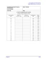
Page 598: ...15 1 15 Safety and Regulatory Information ...

Page 599: ...disconnect the analyzer from mains before cleaning Use a dry cloth or one slightly dampened with water to clean the external case parts Do not attempt to clean internally Assistance Product maintenance agreements and other customer assistance agreements are available for Agilent Technologies products For any assistance contact your nearest Agilent Technologies Sales and Service Office ...

Page 600: ...nada tel 1 877 894 4414 fax 905 282 6495 Europe tel 31 20 547 2323 fax 31 20 547 2390 Australia tel 1 800 629 485 fax 61 3 9210 5947 New Zealand tel 0 800 738 378 fax 64 4 495 8950 Japan tel 81 426 56 7832 fax 81 426 56 7840 Singapore tel 1 800 375 8100 fax 65 836 0252 Malaysia tel 1 800 828 848 fax 1 800 801 664 India tel 1 600 11 2929 fax 000 800 650 1101 Hong Kong tel 800 930 871 fax 852 2506 9...

Page 601: ... attention to a procedure that if not correctly performed or adhered to would result in damage to or destruction of the instrument Do not proceed beyond a caution note until the indicated conditions are fully understood and met WARNING Warning denotes a hazard It calls attention to a procedure which if not correctly performed or adhered to could result in injury or loss of life Do not proceed beyo...

Page 602: ...ion symbol The product is marked with this symbol when it is necessary for the user to refer to the instructions in the documentation The CE mark is a registered trademark of the European Community If accompanied by a year it is when the design was proven The CSA mark is a registered trademark of the Canadian Standards Association This is a symbol of an Industrial Scientific and Medical Group 1 Cl...

Page 603: ... a protective earth contact Any interruption of the protective conductor inside or outside the instrument is likely to make the instrument dangerous Intentional interruption is prohibited WARNING Always use the three prong AC power cord supplied with this product Failure to ensure adequate earth grounding by not using this cord may cause product damage Before Applying Power CAUTION The front panel...

Page 604: ...ING Adjustments described in this document may be performed with power supplied to the product while protective covers are removed Energy available at many points may if contacted result in personal injury WARNING Danger of explosion if battery is incorrectly replaced Replace only with the same or equivalent type recommended Discard used batteries according to manufacturer s instructions WARNING T...

Page 605: ... must be less than the maximum operating temperature of the product by 4 C for every 100 watts dissipated in the cabinet If the total power dissipated in the cabinet is greater that 800 watts then forced convection must be used WARNING Install the instrument according to the enclosure protection provided This instrument does not protect against the ingress of water This instrument protects against...

Page 606: ...eck 7 8 external source mode 12 20 frequency offset 12 19 harmonic analysis 12 19 high band theory 12 17 low band theory 12 15 operation in other modes 12 19 source 12 15 super low band theory 12 15 theory of operation 12 3 tuned receiver mode 12 22 A4 sampler mixer 12 27 A4 sampler mixer check 7 8 A5 sampler mixer 12 27 A6 sampler mixer 12 27 A7 pulse generator check 7 25 A7 pulse generator sourc...

Page 607: ...er 14 42 A21 test port couplers 14 40 A22 test port couplers 14 40 A23 LED board 14 44 A24 transfer switch 14 46 A25 test set interface 14 48 A26 high stability frequency reference 14 50 A3 source 14 18 A4 R sampler 14 20 A5 A sampler 14 20 A6 B sampler 14 20 A7 pulse generator 14 20 A8 post regulator 14 22 A9 CPU 14 24 A9BT1 battery 14 26 B1 fan 14 52 covers 14 6 display 14 12 display lamp 14 12 ...

Page 608: ...on test 2 72 2 75 configurable test set option 1 8 connection techniques 1 7 connector care of 1 7 CONTINUE TEST 10 6 controller GPIB address 4 8 controller troubleshooting 4 9 conventions for symbols 10 42 correction constants ADC offset test 52 3 15 analog bus test 46 3 9 cavity oscillator frequency test 54 3 26 display intensity test 45 6 7 IF amplifier test 51 3 14 initialize EEPROMs test 58 3...

Page 609: ...spur avoidance tracking adjustment 3 52 error BATTERY FAILED STATE MEMORY CLEARED 10 44 BATTERY LOW STORE SAVE REGS TO DISK 10 44 CALIBRATION ABORTED 10 44 CALIBRATION REQUIRED 10 44 CORRECTION CONSTANTS NOT STORED 10 44 CORRECTION TURNED OFF 10 44 CURRENT PARAMETER NOT IN CAL SET 10 45 DEADLOCK 10 45 DEVICE not on not connected wrong addrs 10 45 DISK not on not connected wrong addrs 10 45 DISK HA...

Page 610: ...nter 1 3 10 20 output in SRC tune mode 7 9 range and accuracy test 2 14 2 96 range of fractional N adjustment 3 40 range external source mode test 2 17 2 98 response test 2 36 2 122 front panel digital control 12 11 probe power voltages 5 17 processor digital control of 12 11 troubleshooting 6 12 front panel key codes 6 13 functional group fault isolation 4 10 theory of operation 12 5 fuse check 5...

Page 611: ...REF line 7 18 L HB and L LB Lines 7 18 L INTCOP as trigger to observe control lines 8 8 L INTCOP as trigger to observe data lines 8 8 L LB and L HB Lines 7 18 L LB and L HB lines 7 19 LED front panel 12 25 light occluder 1 3 LIMITS NORM SPCL 10 6 line fuse check 5 7 line voltage check 5 7 LO 2ND waveforms 7 17 LO OUT waveform at A14J2 7 22 load match ELF and ELR 11 10 location diagnostic LEDs for ...

Page 612: ...nd Alter switch position adjustment 3 6 NOT ALLOWED DURING POWER METER CAL 10 46 number option adjustment 3 32 number serial adjustment 3 31 O offset ADC adjustment 3 15 open loop compared to phase locked output in SRC mode 7 10 operating temperature check 5 12 operation check of A9 CPU 6 5 operation verification post repair 3 3 14 53 operator s check 4 6 option numbers correction constants adjust...

Page 613: ...Port 2 Op Chk 10 10 port performance test 2 50 2 131 POSSIBLE FALSE LOCK 10 47 Post Reg 10 9 post regulator air flow detector 12 8 display power 12 8 green LEDs 12 7 probe power 12 8 shutdown circuit 12 8 test point locations 5 6 theory of operation 12 7 variable fan circuit 12 8 post repair procedures 3 3 power from source 7 5 power level accuracy test 2 19 2 100 power linearity test 2 22 2 102 2...

Page 614: ...00 reflection test port output power linearity test 2 102 2 108 removing the line fuse 5 7 repair procedure 4 2 REPEAT ON OFF 10 6 replaceable parts cables 13 32 13 34 cables 8753ES 13 20 13 22 13 26 13 30 cables 8753ET 13 18 13 24 13 28 chassis 13 56 13 58 documentation 13 59 front panel assembly 13 36 13 38 hardware 13 46 13 48 13 49 13 50 13 51 13 52 13 53 13 54 13 55 major assemblies 8753ES 13...

Page 615: ...0 12 Source Def source default test 10 12 SOURCE PLL ON OFF 10 17 SOURCE POWER TURNED OFF RESET UNDER POWER MENU 10 49 source external 1 3 specifications instrument 2 2 system 2 2 spectrum analyzer 1 3 speed fan 5 19 spikes display acceptable versus excessive 3 53 SPUR AVOID ON OFF 10 19 spur avoidance and FM sideband adjustment 3 49 spur avoidance tracking adjustment 3 52 spur search with a filte...

Page 616: ... peripheral equipment 12 4 power supply 12 6 power supply shutdown 12 7 preregulator voltages 12 7 probe power 12 8 receiver 12 4 12 27 signal separation 12 25 source attenuator 12 4 test set 12 4 variable fan circuit 12 8 tool kit 1 3 tools for service 1 2 trace noise test 2 56 2 136 trace with sampler correction on and off 8 10 tracking for source spur avoidance adjustment 3 52 transfer switch 1...

Page 617: ...age differences with SOURCE PLL OFF 7 12 voltages for post regulator 5 6 voltmeter 1 3 VRAM bank 10 13 VRAM video 10 13 W warranty explanation 4 4 waveform integrity in SRC tune mode 7 9 wrist strap and cord antistatic 1 2 WRONG DISK FORMAT INITIALIZE DISK 10 49 Y YO and YO coil drive voltage differences with SOURCE PLL OFF 7 12 YO coil drive check with analog bus 7 11 ...

Reviews: