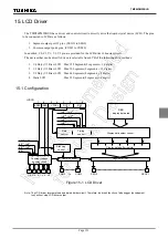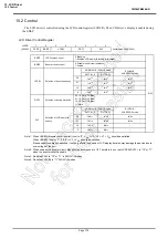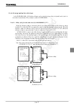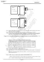
Page 152
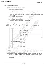
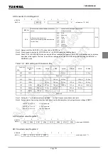
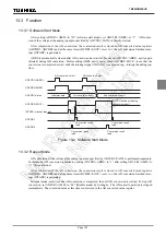
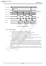
14. Key-on Wakeup (KWU)
14.3 Function
TMP86PM29BUG
Also, each level of the STOP2 to STOP5 pins can be confirmed by reading corresponding I/O port data register,
check all STOP2 to STOP5 pins "H" that is enabled by STOPCR before the STOP mode is started (Note2,3).
Note 1: When the STOP mode released by the edge release mode (SYSCR1<RELM> = “0”), inhibit input from STOP2 to
STOP5 pins by Key-on Wakeup Control Register (STOPCR) or must be set "H" level into STOP2 to STOP5 pins
that are available input during STOP mode.
Note 2: When the
STOP
pin input is high or STOP2 to STOP5 pins input which is enabled by STOPCR is low, executing an
instruction which starts STOP mode will not place in STOP mode but instead will immediately start the release
sequence (Warm up).
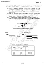
Note 3: The input circuit of Key-on Wakeup input and Port input is separated, so each input voltage threshold value is dif-
ferent. Therefore, a value comes from port input before STOP mode start may be different from a value which is
detected by Key-on Wakeup input (Figure 14-2).
Note 4:
STOP
pin doesn’t have the control register such as STOPCR, so when STOP mode is released by STOP2 to
STOP5 pins,
STOP
pin also should be used as STOP mode release function.
Note 5: In STOP mode, Key-on Wakeup pin which is enabled as input mode (for releasing STOP mode) by Key-on
Wakeup Control Register (STOPCR) may generate the penetration current, so the said pin must be disabled AD
conversion input (analog voltage input).
Note 6: When the STOP mode is released by STOP2 to STOP5 pins, the level of
STOP
pin should hold "L" level (Figure
14-3).
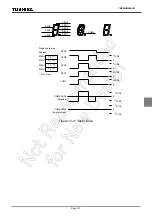
Figure 14-2 Key-on Wakeup Input and Port Input
Figure 14-3 Priority of
STOP
pin and STOP2 to STOP5 pins
Table 14-1 Release level (edge) of STOP mode
Pin name
Release level (edge)
SYSCR1<RELM>="1"
(Note2)
SYSCR1<RELM>="0"
STOP
"H" level
Rising edge
STOP2
"L" level
Don’t use (Note1)
STOP3
"L" level
Don’t use (Note1)
STOP4
"L" level
Don’t use (Note1)
STOP5
"L" level
Don’t use (Note1)
Port input
External pin
Key-on wakeup
input
STOP pin
a) STOP
Release
STOP mode
STOP mode
STOP pin "L"
b)
Release
STOP mode
STOP mode
In case of STOP2 to STOP5
STOP2 pin
Содержание TLCS-870/C Series
Страница 1: ...8 Bit Microcontroller TLCS 870 C Series TMP86PM29BUG ...
Страница 6: ...TMP86PM29BUG ...
Страница 7: ...Revision History Date Revision 2007 10 11 1 First Release 2008 8 29 2 Contents Revised ...
Страница 9: ......
Страница 15: ...vi ...
Страница 19: ...Page 4 1 3 Block Diagram TMP86PM29BUG 1 3 Block Diagram Figure 1 2 Block Diagram ...
Страница 23: ...Page 8 1 4 Pin Names and Functions TMP86PM29BUG ...
Страница 48: ...Page 33 TMP86PM29BUG ...
Страница 49: ...Page 34 2 Operational Description 2 3 Reset Circuit TMP86PM29BUG ...
Страница 61: ...Page 46 3 Interrupt Control Circuit 3 8 External Interrupts TMP86PM29BUG ...
Страница 81: ...Page 66 6 Watchdog Timer WDT 6 3 Address Trap TMP86PM29BUG ...
Страница 135: ...Page 120 10 8 Bit TimerCounter TC5 TC6 10 1 Configuration TMP86PM29BUG ...
Страница 145: ...Page 130 11 Asynchronous Serial interface UART 11 9 Status Flag TMP86PM29BUG ...
Страница 165: ...Page 150 13 10 bit AD Converter ADC 13 6 Precautions about AD Converter TMP86PM29BUG ...
Страница 183: ...Page 168 15 LCD Driver 15 4 Control Method of LCD Driver TMP86PM29BUG ...
Страница 201: ...Page 186 18 Electrical Characteristics 18 9 Handling Precaution TMP86PM29BUG ...
Страница 203: ...Page 188 19 Package Dimensions TMP86PM29BUG ...
Страница 205: ......

