135
TA-DA9000ES
•
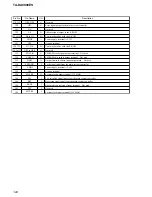
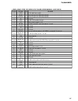
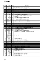
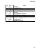
I. LINK BOARD IC3012 TMS320VC5409PGE100A (I. LINK DSP)
Pin No.
Pin Name
I/O
Description
1
VSS
—
Ground terminal
2
A22
O
Address signal output terminal Not used
3
VSS
—
Ground terminal
4
DVDD (3.3V)
—
Power supply terminal (+3.3V)
5
A10
O
Address signal output terminal Not used
6
HD7
I/O
Two-way data bus with the i. link system controller
7 to 11
A11 to A15
O
Address signal output terminal Not used
12
CVDD (1.8V)
—
Power supply terminal (+1.8V)
13
HAS
I
Address strobe signal input from the i. link system controller
14, 15
VSS
—
Ground terminal
16
CVDD (1.8V)
—
Power supply terminal (+1.8V)
17
HCS
I
Chip select signal input from the i. link system controller
18
HR/W
I
Read/write signal input from the i. link system controller
19
READY
I
Ready signal input terminal Not used
20
PS
I
Program select signal input terminal Not used
21
DS
I
Data select signal input terminal Not used
22
IS
I
I/O space select signal input terminal Not used
23
R/W
O
Read/write signal output terminal Not used
24
MSTRB
O
Memory strobe signal output terminal Not used
25
IOSTRB
O
I/O strobe signal output terminal Not used
26
MSC
O
Microstate complete signal output terminal Not used
27
XF
O
External flag signal output to the i. link system controller
28
HOLDA
O
Hold acknowledge signal output terminal Not used
29
IAQ
O
Instruction acquisition signal output terminal Not used
30
HOLD
I
Hold signal input terminal Not used
31
BIO
I
Branch control signal input terminal Not used
32
MP/MC
I
Microprocessor/microcomputer mode selection signal input terminal
“L”: microcomputer mode, “H”: microprocessor mode Fixed at “L” in this set
33
DVDD (3.3V)
—
Power supply terminal (+3.3V)
34
VSS
—
Ground terminal
35
BDR1
I
Serial data input terminal Not used
36
BFSR1
I
Frame sync signal input terminal Not used
37
VSS
—
Ground terminal
38
BCLKR1
I
Receive clock signal input terminal Not used
39
HCNTL0
I
Control signal input from the i. link system controller
40
VSS
—
Ground terminal
41, 42
BCLKR0, BCLKR2
I
Receive clock signal input terminal Not used
43, 44
BFSR0, BFSR2
I
Frame sync signal input terminal Not used
45
BDR0
I
Serial data input terminal Not used
46
HCNTL1
I
Control signal input from the i. link system controller
47
BDR2
I
Serial data input terminal Not used
48, 49
BCLKX0, BCLKX2
I
Transmit clock signal input terminal Not used
50
VSS
—
Ground terminal
51
HINT/TOUT1
O
Interrupt signal output to the INT2 (
yh
pin)
52
CVDD (1.8V)
—
Power supply terminal (+1.8V)
Содержание TA-DA9000ES
Страница 16: ...16 TA DA9000ES 3 10 MOTHER BOARD 1 four screws transistor 3 mother board 2 heat sink ...
Страница 22: ...MEMO TA DA9000ES 22 ...
Страница 193: ...193 TA DA9000ES MEMO ...


