139
TA-DA9000ES
•
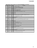
AMP BOARD IC1800 MB89537APFM-G-461-BNDE1 (OUTPUT CONTROLLER)
Pin No.
Pin Name
I/O
Description
1
4/8 IN
I
Current detection signal input from the protect circuit
2
MOD2
I
Not used
3
TEMP
I
Temperature detection signal input from the thermistor
4 to 10
—
—
Not used
11
AVCC
—
Power supply terminal (+3.3V)
12
AVR
I
Reference voltage (+3.3V) input terminal
13
AVSS
—
Ground terminal
14
U-MAIN
I
Clock signal input from main system controller
15
AC-OFF
I
AC off detection signal input terminal “L”: AC off
16 to 18
—
—
Not used
19
RST
I
System reset signal input from the main system controller “L”: reset
20, 21
MOD0, MOD1
I
Setting terminal for memory access mode Normally: fixed at “L”
22
X0
I
System clock input terminal (8 MHz)
23
X1
O
System clock output terminal (8 MHz)
24
VSS
—
Ground terminal
25
VOL-CLK
O
Serial data transfer clock signal output to the data decoder
26
VOL-DATA
O
Serial data output to the data decoder
27
VOL-LAT
O
Serial data latch pulse signal output to the data decoder
28
DAC-MUTE
O
Muting on/off control signal output terminal “H”: muting on
29, 30
(P23), (P22)
—
Not used
31
4I-LIMIT
I
IMPEDANCE SELECTOR switch input terminal “L”: 4
Ω
, “H”: 8
Ω
32
DC
I
DC off detection signal input terminal
33
I LIMIT
I
Current detection signal input terminal Not used
34
4/8OUT
O
Relay drive signal (for speaker impedance 4
Ω
/8
Ω
selection) output terminal
35
DIAG
I
Temperature detection signal input from the power amplifier
36
EN
O
Enable signal output terminal
37
MODE1
O
PCM/DSD data selection signal output terminal Not used
38
INIT
O
Initialize signal output to the PCM/PWM processor
39
NSP-MUTE
O
Muting on/off control signal output terminal Not used
40
(P10)
—
Not used
41
—
—
Not used
42
U-SUB1
I
Serial data input from main system controller
43
LAT4
O
Serial data latch pulse signal (for surround back) output to the PCM/PWM processor
44
LAT3
O
Serial data latch pulse signal (for surround) output to the PCM/PWM processor
45
LAT2
O
Serial data latch pulse signal (for center) output to the PCM/PWM processor
46
LAT1
O
Serial data latch pulse signal (for front) output to the PCM/PWM processor
47
F-B RY
O
Relay drive signal (for front speaker B) output terminal
48
SR-A RY
O
Relay drive signal (for surround speaker A) output terminal
49
NC
—
Not used
50
F-A RY
O
Relay drive signal (for front speaker A) output terminal
51
SHIFT
O
Serial data transfer clock signal output to the PCM/PWM processor
52
SO1/SCDT
O
Serial data output to the PCM/PWM processor
53
SI1/SR-B RY
O
Relay drive signal (for surround speaker B) output terminal
54
C RY
O
Relay drive signal (for center speaker) output terminal
55
SB RY
O
Relay drive signal (for surround back speaker) output terminal
Содержание TA-DA9000ES
Страница 16: ...16 TA DA9000ES 3 10 MOTHER BOARD 1 four screws transistor 3 mother board 2 heat sink ...
Страница 22: ...MEMO TA DA9000ES 22 ...
Страница 193: ...193 TA DA9000ES MEMO ...


