2-11
Operations & Installation
2-2-2 Camp On Busy
(Available only when you have more than one handset)
This feature allows your handset to wait for connection to the telephone line currently engaged by another
handset. Your handset rings when the telephone line becomes free.
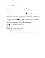
1. You hear a short busy tone if you open the flip cover or press
key while another handset engages the
telephone line.
The display shows the handset number currently engaging the line. Your handset is automatically camped
on the line.
Note:
To cancel this feature, press
key any time before the line is free. The handset returns to Standby
mode.
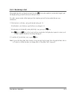
2. Your handset rings and the window displays
FREE
when the line becomes free.
3. Press
key to engage the line while the handset rings.
Notes:
¥ If an incoming call arrives while your handset rings to tell you the line is free, the ÔCamp On BusyÕ feature is
automatically cancelled and an incoming ring sounds.
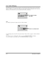
¥ Several handsets can be camped on the busy line in
chronological order. When the line becomes available to you, the LCD window displays
FREE
, and other
handsets will display your handset number following the word
BUSY
.
¥ When your handset rings and the window displays
FREE
, press the key within 10 seconds. Otherwise, the
handset returns to the Standby mode.
Содержание SP-R6100
Страница 3: ......
Страница 50: ...Exploded View Parts List 3 4 3 4 SP R6100 BASE Exploded View 1 7 8 9 10 13 14 15 16 2 3 11 9 12 4 5 6 ...
Страница 52: ...Exploded View Parts List 3 6 3 6 SP R6100 CHARGER Exploded View 6 8 7 1 2 3 4 5 9 ...
Страница 54: ...Exploded View Parts List 3 8 SP R6100 PACKING Exploded View 3 8 3 7 4 1 5 8 2 6 9 ...
Страница 67: ...6 1 6 PCB Diagrams 6 1 SP R6100 Base PCB I ...
Страница 68: ...PCD Diagrams ...
Страница 69: ...6 2 SP R6100 Base PCB II 6 2 ...
Страница 70: ...PCD Diagrams ...
Страница 71: ...6 3 SP R6100 Handy PCB I 6 3 ...
Страница 72: ...PCD Diagrams ...
Страница 73: ...6 4 SP R6100 Handy PCB II 6 4 ...
Страница 74: ...PCD Diagrams ...
Страница 75: ...6 5 SP R6100 Key PCB I PCD Diagrams 6 5 ...
Страница 76: ...6 6 SP R6100 Key PCB II PCB Diagrams 6 6 ...
Страница 77: ...6 7 SP R6100 Charger PCB I 6 7 PCD Diagrams ...
Страница 78: ...6 8 SP R6100 Charger PCB II PCB Diagrams 6 8 ...
Страница 79: ...Schematic Diagrams 7 1 7 Schematic Diagrams 7 1 SP R6100 Hand LOGIC ...
Страница 80: ...Schematic Diagrams 7 2 7 2 SP R6100 Hand RF SL18 9 SL55 SL18 9 SL19 SL7 SL9 5 SL18 9 SL18 9 SL5 5 SL7 5 SL5 ...
Страница 81: ...Schematic Diagrams 7 3 7 3 SP R6100 BASE LOGIC ...
Страница 82: ...Schematic Diagrams 7 4 7 4 SP R6100 Base CLIP ...
Страница 84: ...Schematic Diagrams 7 6 HAND KEY 7 6 ...
Страница 85: ...Schematic Diagrams 7 7 CHRGER 7 7 ...
Страница 88: ...Samsung Electronics Co Ltd ELECTRONICS ...


