5.8.2 Power Supply.
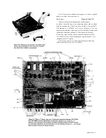
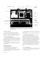
Check the power supply (V assembly) if there is a massive failure
(nothing works) or as a starting procedure in any thorough analysis. Refer
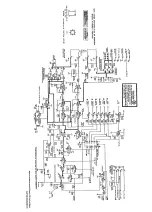
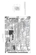
to figures 5-8 and 6-10.
NOTE
If a power transistor (U1, U2, or U3) must be replaced, be sure to
spread silicone grease
(like Dow Corning compound no. 5) on the
surface toward the heat sink. For U 1, coat
both sides of the insulating washer.
a. Check the output voltages, using a digital voltmeter, with ground
reference at V-J1, pin 9 (ribbon cable unplugged), as follows:
Pin1=+5V.
Pin3=+5V.
Pin4=-8V.
b. Make a check similar to step a, with ribbon cable connected, ground
reference at right edge of C board, probing C-J1 from below the board. (This
checks for overload outside the power supply.)
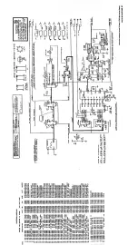
5.8.3 Sinewave Generator. Figure 6-5.
Check the C-board circuits that supply the test signal
to the DUT, as follows: (We proceed backward, toward the si newave
generator.)
a. Make the following test setup and pushbutton
selections:
DUT: 0.1 uF and 3 k
Ω
, connected in series.
FREQUENCY: 1 kHz.
PAR SERIES: SERIES.
FUNCTION: C/D.
RANGE: 2.
b. Verify that the signal at test fixture I+ (Figure 6-4) is a
1-kHz sine wave, 0.6 V pk-pk. Use an oscilloscope.
c. Verify that this signal changes amplitude as you
switch ranges, thus:
RANGE 1, 0.68 V pk.pk;
RANGE 3, 20 mV pk-pk.
d. If no fault appears in steps a, b, c, skip to para 5.8.4.
e. Verify that "0.25 V RMS TEST SIGNAL" found at S03 pin 14 is a 1-
kHz sine wave, approx 0.6 V pk-pk. (+/-15%). This is the output from U41
pin 6.
f. Check at U41 pin 3 (the pin closest to the front) for
a 1-kHz sine wave, 0.4 V pk-pk.
g. Verify that the output of U 18 found at S03 pin 5 is a 1-kHz sine
wave, 0.8 V pk-pk. (It is rather noisy, as sketched on the schematic diagram,
Figure 6-5.)
h. Remove U 18. Connect a 200-
Ω
resistor across its socket (XU18)
between pins 2 and 3. (Note: if the resistor leads are about 0.5 mm [0.02 in.]
in diameter,
aa
. If trouble is found at step a, check
"+5
V" circuit: At outputs of U1
and U2:
+5
V dc (regulated).
At WT1 (inputs of U1 and U2): +10.8 V dc.
Across input to diode bridge (yellow-to-yellow): 10 V rms.
ab
.Check
"-8
V" circuit:
At output of U3:
-8
V dc (regulated).
At input (center terminal) of U3:
-13.8
V dc.
Across WT7 to WT8:
11.3
V rms.
ac.
Check power-line circuit to primary of transformer V-T1.
ca
. If this signal is distorted
or
missing on all ranges, but present at
the right end of R 103, check diode network C-CR
16
...CR23. If missing
on some ranges(s), check source resistor circuit R101... R103
and switches S1... S3.
fa
. Check at U45 pin 10 for a 1-kHz sine wave, 60
m
V pk-pk. If this is
verified but step e is not, fault is in U41.
5-12 SERVICE
Содержание 1657 RLC Digibridge
Страница 6: ...Table of Contents...
Страница 8: ...1 2 INTRODUCTION...
Страница 9: ...INTRODUCTION 1 3...
Страница 10: ...1 4 INTRODUCTION...
Страница 15: ...OPERATION 3 1...
Страница 24: ...4 2 THEORY...
Страница 30: ...5 4 SERVICE...
Страница 42: ...5 16 SERVICE...
Страница 46: ......
Страница 49: ......
Страница 50: ......
Страница 51: ......
Страница 52: ......
Страница 53: ......
Страница 54: ......
Страница 55: ......
Страница 56: ......
Страница 57: ......

