background image

502 069 02

Manual

Power Monitor, PD 3260

35/79

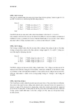
SWNo $AB: FullScale.

FullScale is a record having the following structure:

Record

Current: Real;

(* FullScale for current inputs *)

(* Offset = 0 *)

VoltageU: Real;

(* FullScale for Voltage.U input *)

(* Offset = 4 *)

VoltageV: Real;

(* FullScale for Voltage.V input *)     (* Offset = 8 *)

VoltageW: Real;

(* FullScale for Voltage.W input*)

(* Offset = 12 *)

End;

FullScale.Current is a common fullscale for the current inputs. The current inputs are calibrated

to be identical, so the chosen current mesurement transformers must be of the same type and ratio.

FullScale.VoltageU, FullScale.VoltageV and FullScale.VoltageW, are separate fullscale values

for the voltage inputs. The FullScale values can be written directly to the variables or they can be

calculated automatically. Automatic calculation is disabled when the channel is in input

simulation mode.

Example: A 10:1 ratio current transformer is selected to match the current to be measured, with

the nominal 1A RMS input current of the module.

The 10A RMS primary current needed to give 1A RMS at the  input of the module, can be written

directly into FullScale.Current. The value of FullScale.Current can also be calculated automati-

cally, by writing the readout of a reference amperemeter, connected in series with the primary of

the transformer in L1, into the Current.U variable. The calibration current used for automatic

calculation of fullscale, should be larger than 20% of fullscale. 

Example: A 230:24 ratio voltage transformer is selected to match the voltage to be measured,

with the nominal 24V RMS input voltage of the module.

The 230V RMS primary voltage needed to give 24V RMS at the input of the module, can be

written directly to the FullScale.VoltageU/V/W variables. The fullscale values for the voltage

inputs can also be calculated automatically, by writing  the readout of a reference voltmeter

connected to the primary side of the measurement transformer, to the corresponding

Voltage.U/V/W variables. The calibration voltage should be a reasonable fraction of fullscale.

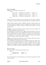
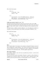
SWNo $AC: Factors.

The factors variable is a record having the following structure:

Record

PowerScale: Real;

(* Offset = 0 *)

EnergyScale: Real;

(* Offset = 4 *)

End;

The Factors variables, PowerScale and EnergyScale, are unit conversion factors for the readout

of power and energy.

Содержание PD 3260 PMM

Страница 1: ...502 069 02 GB February 1997 PROCES DATA A S Navervej 8 8600 Silkeborg Denmark Phone 45 87 200 300 fax 45 87 200 301 POWER MONITOR MODULE PD 3260 PMM Manual ...

Страница 2: ...or PD 3260 Manual Copyright 1997 by PROCES DATA A S All rights reserved PROCES DATA A S reserves the right to make any changes without prior notice P NET Soft Wiring and Process Pascal are registered trademarks of PROCES DATA A S ...

Страница 3: ...erator Switch Channel channel B 41 6 1 Connections to Generator Switch Channel 49 7 Thyristor Switch Channel channel C 51 7 1 Connections to Thyristor Switch Channel 57 8 Calculator program 58 9 Program Channel channel D 59 10 Data Channel channel E 71 11 Construction Mechanical 74 12 Specifications 75 12 1 Power supply 75 12 2 Digital Input 75 12 3 Digital Output 75 12 4 Power Monitor 76 12 5 Gen...

Страница 4: ...502 069 02 IV IV Power Monitor PD 3260 Manual ...

Страница 5: ...for process control and data collection The PD 3260 module has been developed to directly interface with digital process signals Configuration of the module for the functions required and communication between the module and a control computer is carried out via the P NET fieldbus The PD 3260 module can be controlled via P NET or it can operate as an autonomous unit The module possesses a programm...

Страница 6: ...rent and voltage inputs can be enabled Total effective power is calculated and the level can be monitored by enabling user presettable HighLevel and LowLevel alarms In addition the total effective power is integrated over time to provide Total Produced and Consumed Energy values The line frequency is continuously measured Generator Switch Channel The Generator Switch channel can be used to connect...

Страница 7: ...de overload is generated in the module The common I O channel in the module provides the ability to read set all inputs outputs using a single P NET transmission General The unit offers comprehensive self testing features which enables the reporting of disconnection overload and process failure All outputs are protected against overload The watchdog timer ensures the safe shut down of a process fo...

Страница 8: ...1 Data channel channel 0E A set of 16 variables numbered from 00 0F is associated with each channel For addressing a variable within a particular channel a logical address called a SoftWire Number SWNo is used The SWNo is calculated as channel number 10 variable number within the channel Example Variable 4 on channel 3 needs to be addressed The SWNo will therefore be 34 Throughout the manual the v...

Страница 9: ... reversed connections Connection identities are printed on the top of the module The module wiring should be designed with a maximum of 2 wire connections in each screw terminal The module has a built in fuse which is used to protect the module and externally connected wiring and equipment When connecting exter nal equipment the additional fuse protected 24 V screw terminals should be used see har...

Страница 10: ...tile type The following memory types are listed in the channel definition tables Read Only PROM ReadOnly The PROM is always write protected and can never be changed RAM ReadOnly The variable is stored in RAM and is only accessible for Reading Read Protected Write EEPROM RPW Read Protected Write The EEPROM is always write protected directly following a reset By setting WriteEnable to TRUE the conte...

Страница 11: ...n RAM If WriteEnable is TRUE the value is changed in both RAM and EEPROM when the variable is modified via P NET RAM AutoSave Has the same function as RAM InitEEPROM with the addition that the contents of RAM are automatically copied to EEPROM at a frequency of approximately 10 hours After copying to EEPROM a new sumcheck value is calculated The new sumcheck value is stored in the EEPROM unless an...

Страница 12: ...teger 8 WDTimer RAM Read Write Decimal Real 9 ModuleConfig EEPROM RPW Record A WDPreset EEPROM RPW Decimal Real B C D WriteEnable RAM Read Write Binary Boolean E ChType PROM Read Only Record F CommonError RAM Read Write Record SWNo 0 NumberOfSWNo This variable holds the highest SWNo in the module SWNo 1 DeviceID The purpose of this record is to be able to identify the device The record includes a ...

Страница 13: ...NET is performed by writing the required node address together with the serial number of the module in question into the PnetSerialNo at node address 7E calling all modules All modules on the P NET will receive the message but only the module with the transmitted serial number will store the P NET node address An attempt to write data to node address 7E will give no reply Consequently the calling ...

Страница 14: ...Functions 0 Watchdog ModuleConfig Functions 10 No watchdog SWNo A WDPreset s The maximum time allowable between two calls to the module before the watchdog is activated is defined in this register in seconds SWNo D WriteEnable Write protected variables can only be changed when WriteEnable is TRUE After reset WriteEnable is set to FALSE After modifying the contents of module EEPROM WriteEnable shou...

Страница 15: ...ber for the channel type and a TRUE boolean value for each of the registers which are represented within a channel The register number in a channel corresponds to the index number in the boolean array In addition to these fields various other fields can be found in the record the contents of which depends on the channel type The record for the service channel has the following structure Record Cha...

Страница 16: ...able holds error information on all Channels This variable is a record having the following structure Record ChError Record His Array 0 7 of Boolean Offset 0 Act Array 0 7 of Boolean Offset 2 End ComHis16 Array 0 15 of Boolean Offset 4 ComAct16 Array 0 15 of Boolean Offset 6 End The 8 bits in ChError His and ChError Act have the following meaning 7 6 5 4 3 2 1 0 InternalReset Hardware ExternalRese...

Страница 17: ...ponding bits in ChError Act and ChError His is set 2 When the error disappears the corresponding bit is reset in ChError Act 3 After reading ChError His ChError Act is copied to ChError His 4 Transmission responses from a module will include the Actual Data Error bit DataError set TRUE if ChError Act 0 5 The Historical Data Error bit GeneralError will be set TRUE in all responses from the module i...

Страница 18: ...l D Program Ch Channel C Thyristor Sw Channel B Generator Sw Channel A Power monitor Channel 9 Common I O Channel 8 Digital I O 8 Channel 7 Digital I O 7 Channel 6 Digital I O 6 Channel 5 Digital I O 5 Channel 4 Digital I O 4 Channel 3 Digital I O 3 Channel 2 Digital I O 2 Channel 1 Digital I O 1 Channel 0 Service Channel ...

Страница 19: ...B Preset EEPROM RPW Decimal Real s x8 OutPreset EEPROM RPW Decimal Real s x9 ChConfig EEPROM RPW Record xA MinCurrent EEPROM RPW Decimal Real A xB MaxCurrent EEPROM RPW Decimal Real A xC UserRealArray EEPROM RPW Array2Real xD Maintenance EEPROM RPW Record xE ChType PROM Read Only Record xF ChError RAM Read Only Binary Record SWNo x0 FlagReg 7 6 5 4 3 2 1 0 OutFlag InFlag InAFlag InBFlag Control FB...

Страница 20: ...BFlag is identical to the input flag for the channel selected as Feedback input B Feedback input B is the input signal which should correspond with the inverse state of the output signal This input signal is selected in ChConfig Ref_B The feedback signals can be simulated by setting ChConfig Enablebit 2 TRUE If feedback simulation is selected the InAFlag and InBFlag are automatically set to the co...

Страница 21: ...ter exceeds 2147483647 it restarts at 2147483648 The counter increments by one every time the InFlag changes from 0 to 1 SWNo x3 OutCurrent A The OutCurrent register indicates the sink current in the output load It is measured with a resolution of approximately 12 mA The stability of the measurement depends on the power supply stability SWNo x4 Operatingtime s This variable totalises the time peri...

Страница 22: ...edback control single or double feedback and a choice of special output functions Feedback control The correct feedback state is Input A Output AND Input B NOT Output The feedback inputs can be disabled by writing a 0 as the channel number in ChConfig Ref_A and or ChConfig Ref_B fields if only one or no input channels are required The ChConfig variable is a record having the following structure Re...

Страница 23: ... OutTimer Output is reset if the Control Flag is set to FALSE and the output may be controlled directly via P NET Precise Function description After reset InternalState False FlagReg Control False Loop If NOT InternalState and FlagReg Control then Positive edge OutTimer OutPreset If InternalState and NOT FlagReg Control then Negative edge FlagReg OutFlag False InternalState FlagReg Control If Flag...

Страница 24: ...ll six outputs are used This function is selected by setting ChConfig Functions 40 in the individual I O channels The thyristor switch channel uses the digital outputs in pairs I O 1 2 I O 3 4 and I O 5 6 Both of the IO s in a pair must be configured otherwise none of them will be used The digital I O 7 and I O 8 cannot be used by the thyristor switch channel When the output is controlled by the T...

Страница 25: ...ON and the FBTimer 0 an error may be generated Error code generation is enabled by setting ChConfig Enablebit 5 TRUE underload alarm Precise Function description If OutCurrent MinCurrent and FlagReg OutFlag true and FBTimer 0 and ChConfig EnableBit 5 then ChError Act UnderLoad true else ChError Act UnderLoad false SWNo xB MaxCurrent A If Outcurrent exceeds MaxCurrent and FBTimer 0 the output is sw...

Страница 26: ... particularly in connection with a calculator program This variable has no effect on the standard functions for a digital I O channel SWNo xD Maintenance The Maintenance variable is used for service management and maintenance purposes and holds the last date of service and an indication of the type of service The Maintenance is a record having the following structure Record Date BYTE Offset 0 Mont...

Страница 27: ...1 1 1 Not used Not used Not used Not used Not used Not used Not used Not used Not used Not used Timer Output Thyristor Switch 50 Duty Cycle output One shot output Output Input only Not implemented in Ch7 and Ch8 Feedback 15 14 13 12 11 10 9 8 7 6 5 4 3 2 1 0 0 0 0 0 0 0 0 0 0 0 0 0 0 0 1 1 Not used Not used Not used Not used Not used Not used Not used Not used Not used Not used Not used Not used N...

Страница 28: ...he individual channels see also Service channel Bit 6 OverLoad is set if the current in the output load exceeds MaxCurrent default 1 A The Overload alarm can be disabled by setting ChConfig Enablebit 6 TRUE ChError Act OverLoad remains set until a Write operation is performed on the FlagReg variable Bit 5 UnderLoad is set if the load is disconnected OutCurrent MinCurrent The Underload alarm can be...

Страница 29: ...s controlled by the Thyristor Switch Channel Bit 1 FeedBackError is set if there is a feedback error see FBTimer Bit 0 PrgError is set following attempts to set FlagReg OutFlag if the I O is configured to be an input or following attempts to set FlagReg Control if the I O is configured to be an input or an output without any automatic functions ChError Act PrgError remains set until a Write operat...

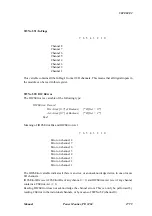
Страница 30: ...99 9A 9B 9C 9D 9E ChType PROM Read Only Record 9F ChError RAM Read Only Binary Record SWNo 90 OutFlags 7 6 5 4 3 2 1 0 Channel 8 Channel 7 Channel 6 Channel 5 Channel 4 Channel 3 Channel 2 Channel 1 This variable contains all the OutFlag s from all I O channels This means that all digital outputs in the module can be controlled from this register NOTE When setting an outflag TRUE via the Common I ...

Страница 31: ...0 7 of Boolean Offset 2 End Meaning of IOChError His and IOChError Act 7 6 5 4 3 2 1 0 Error on channel 8 Error on channel 7 Error on channel 6 Error on channel 5 Error on channel 4 Error on channel 3 Error on channel 2 Error on channel 1 The IOChError variable indicates if there is an error or an unacknowledged error in one or more I O channels IOChError His is set if ChError His of any channel 0...

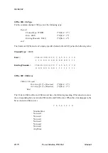
Страница 32: ... 6 5 4 3 2 1 0 1 1 0 0 0 0 0 0 0 0 0 0 0 1 1 1 ExistingChannels 15 14 13 12 11 10 9 8 7 6 5 4 3 2 1 0 0 0 0 0 0 0 0 0 1 1 1 1 1 1 1 1 SWNo 9F CHError ChError Record His Array 0 7 of Boolean Offset 0 Act Array 0 7 of Boolean Offset 2 End The 8 bits in ChError His and ChError Act have the following meaning When an error occurs the corresponding bit is set in both ChError His and ChError Act When the...

Страница 33: ...if there is an error or an unacknowledged error in one or more I O channels ChError His 0 is set if any bit is set in IOChError His indicating any historical error on any I O channel ChError Act 0 is set if any bit is set in IOChError Act indicating any actual error on any I O channel Reading ChError does not acknowledge the channel errors This can only be done by reading ChError in the individual...

Страница 34: ...Produced and Consumed Energy The line frequency is also measured The primary inputs are precision factory calibrated Automatic calculation of fullscale for voltage and current inputs are possible to ease calibration of the module when using current and voltage transformers All variables are represented in engineering units The power and energy variables can be individually scaled for the most appr...

Страница 35: ...n the variable holds the integrated positive and negative power respectively which could be used when a process is both producing and consuming power The readout unit for Energy may be scaled using the Factors EnergyScale variable The energy variables can be cleared or preset by writing new values to the variables SWNo A2 PhasePower The PhasePower variable is only used when the channel is in singl...

Страница 36: ...1 Voltage is a record having the following structure Record U Real RMS voltage line phase L1 Offset 0 V Real RMS voltage line phase L2 Offset 4 W Real RMS voltage line phase L3 Offset 8 End The RMS voltages are measured with voltage transformers The voltage scale factors must be inserted in the FullScale VoltageU V W variables Automatic calculation of the fullscale values is performed if ServiceCh...

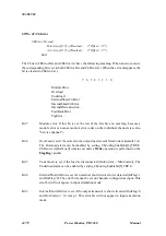
Страница 37: ...arm False SWNo A8 Lowlevel LowLevel is a limit switch for the Power variable having the following function IF Power LowLevel AND ChConfig Enablebit 3 True THEN LowAlarm True ELSE LowAlarm False SWNo A9 ChConfig The channel configuration for the Power Monitor channel is stored in a record having the following structure Record Enablebit Array 0 7 of Boolean Offset 0 Functions BYTE Offset 1 Ref_A BYT...

Страница 38: ...ineFreq variable See also the description for Bit1 in ChError If input simulation is enabled the automatic updating of measured and calculated variables is disabled Any value can be written to the variables for test purposes during commisioning The alarms maintain their normal function but use the simulated values Automatic calculation of fullscale values is disabled Functions The functions field ...

Страница 39: ...input of the module can be written directly into FullScale Current The value of FullScale Current can also be calculated automati cally by writing the readout of a reference amperemeter connected in series with the primary of the transformer in L1 into the Current U variable The calibration current used for automatic calculation of fullscale should be larger than 20 of fullscale Example A 230 24 r...

Страница 40: ...te Offset 0 Month Byte Offset 1 Year Byte Offset 2 Category Byte Offset 3 End The Maintenance variable is used for service management and maintenance purposes and holds the last date of service and indicates the type of service SWNo AE ChType For the Power Monitor channel ChType has the following structure Record ChannelType WORD Offset 0 Exist Bit16 Offset 2 Functions Bit16 Offset 4 End ChType ha...

Страница 41: ...ay 0 7 of Boolean Offset 0 Act Array 0 7 of Boolean Offset 2 End The 8 bits in ChError His and ChError Act have the following meaning When an error occurs the corresponding bit is set in both ChError His and ChError Act When the error disappears the bit is cleared in ChError Act ChError 7 6 5 4 3 2 1 0 Module Error CurrentHigh VoltageHigh HighAlarm Power LowAlarm Power Symmetry Error External Erro...

Страница 42: ...rue Bit 4 HighAlarm is set if Power HighLevel and ChConfig Enablebit 4 True Bit 3 LowAlarm is set if Power LowLevel and ChConfig Enablebit 3 True Bit 2 Symmetry Error is set if the sum of currents is larger than 40 of the value in FullScale Current and one of the currents differs from 1 3 of the sum of currents by more than 20 during 5 periods of the line frequency and ChConfig Enablebit 2 True Bi...

Страница 43: ... mode only two voltage measurement transformers are required to measure the L1 and L2 line voltages referenced to the L3 line which is used as the common for the primary side of the voltage transformers The secondary side of the transformers are all referenced to the 24V terminal on the module The line voltage between the L1 and L2 lines may be measured by a third voltage transformer if required I...

Страница 44: ... are referenced to the 24V terminal on the module It is recommended that unused voltage inputs are connected to the 24V terminal The U1 voltage input must always be used because the frequency measurement is performed using this input The voltage transformers must be chosen to match the phase voltages with the voltage inputs of the module The voltage inputs are high precision factory calibrated The...

Страница 45: ...tween generator and line frequency is less than a configured value Synchronous generator The difference in phase phase speed and phase acceleration between the line voltage and generator voltage is measured to calculate when the phase shift will be zero The generator is connected at this moment in time if the difference between generator and line frequency is less than a configured value The Gener...

Страница 46: ...ecimal Real s BD Maintenance EEPROM RPW Record BE ChType PROM Read Only Record BF ChError RAM Read Only Binary Record SWNo B0 FlagReg 7 6 5 4 3 2 1 0 SwitchEnable OutFlag Not used Not used Not used Not used Not used Not used Bit 7 SwitchEnable The start function is enabled by setting SwitchEnable True When the switching conditions are satisfied the OutFlag is set and the controlled output channel ...

Страница 47: ...de of the switching element See diagram in chapter 6 1 SWNo B2 PhaseSpeed The PhaseSpeed variable holds the phase speed between the generator and line frequency Calculation PhaseSpeed line frequency generator frequency 360 s SWNo B3 PhaseAcc The PhaseAcc variable holds the phase acceleration between the generator and line frequency Calculation PhaseAcc PhaseSpeed OldPhaseSpeed DeltaT s s SWNo B9 C...

Страница 48: ...o simulate any value in a variable for test purposes Input simulation is enabled by setting ChConfig EnableBit 0 to true Functions The functions field is used in a hexadecimal format where the most significant digit is used to specify the channel functions Functions 00 Channel disabled Functions 10 Asynchronous generator switch Functions 20 Synchronous generator switch If the channel is not used t...

Страница 49: ...Precise function description After reset SwitchEnable False OutFlag False Loop IF SwitchEnable True AND ABS PhaseSpeed StartSpeed THEN OutFlag True at calculated time when Phase 0 IF SwitchEnable False THEN OutFlag False End Ref_A Ref_A holds the number of the channel to be controlled If a Digital I O Channel is selected it must be configured as an output Functions 10 If the Thyristor Switch Chann...

Страница 50: ...erators some frequency difference must be allowed otherwise the module may not be able to couple the generator because a zero phase shift between line and generator does not occur within the specified phase speed difference range SWNo BC DelayComp The calculated start time for generator coupling can be modified by inserting a value in the DelayComp variable to compensate for relay contact delay or...

Страница 51: ...s the following value ChannelType 8008 Exist 15 14 13 12 11 10 9 8 7 6 5 4 3 2 1 0 1 1 1 1 1 1 1 0 0 0 0 0 1 1 1 1 Functions 15 14 13 12 11 10 9 8 7 6 5 4 3 2 1 0 0 0 0 0 0 0 0 0 0 0 0 0 0 1 1 1 Not used Not used Not used Not used Not used Not used Not used Not used Not used Not used Not used Not used Not used Synchronous generator Asynchronous generator Channel can be disabled SWNo BF ChError ChE...

Страница 52: ... Module error Not used Not used Not used Not used Not used Switch Error Not used Bit 7 Module Error If this bit is set the rest of the bits have no meaning because a Module error can lead to random error codes on individual channels also see Service channel Bit 1 Switch Error Generator not connected due to the fact that the generator frequency has passed the line frequency by the frequency differe...

Страница 53: ...to the digital I O 8 terminal Any of the remaining 7 I O s may be configured as the controlling output from the Generator Switch Channel Using I O 7 as the output is the best choice since I O 1 to I O 6 can also be used by the Thyristor Switch Channel to perform thyristor triggering Only the voltage transformer between L1 and L2 and the tachometer input are necessary inputs for the asynchronous ge...

Страница 54: ...to the generator terminal UGEN The primary of the transformer must be connected between the L1 and L3 lines in a similar way to the line voltage transformer between L1 and L3 but on the other side of the switching element Only the voltage transformers connected between L1 and L3 on the power line and at the generator are nessecary inputs for the synchronous generator switch function Additional cur...

Страница 55: ...for the Thyristor Switch Channel Variables on Thyristor Switch channel Channel identifier ThyristorSwitch SWNo Identifier Memory type Read out Type SI Unit C0 FlagReg RAM Read Write Binary Array C1 TrigAngle RAM Read Write Decimal Real C2 C3 C4 C5 C6 TrigSlope RAM Init EEPROM Decimal Real s C7 C8 C9 ChConfig EEPROM RPW Record CA CB TrigMax RAM Init EEPROM Decimal Real CC TrigMin RAM Init EEPROM De...

Страница 56: ... the diagram below The thyristor coupling angle is the output from the ramp and can be read in the TrigAngle variable The ramp function is enabled or disabled with the TrigEnable bit in the FlagReg variable Up or down ramping is controlled by the sign of the TrigSlope variable SWNo C0 FlagReg 7 6 5 4 3 2 1 0 TrigEnable Not used Not used Not used Not used Not used Not used Not used Bit 7 TrigEnable...

Страница 57: ...EN TrigAngle TrigMin END ELSE Thyristors Off END Loop SWNo C6 TrigSlope TrigSlope holds the slope of the thyristor coupling ramp The ramp slope is measured in deg s Up ramping is obtained by writing a positive value in the TrigSlope variable SWNo C9 ChConfig The channel configuration for the Thyristor Switch Channel is stored in a record having the following structure Record Enablebit Array 0 7 of...

Страница 58: ...he digital outputs in pairs I O 1 I O 2 I O 3 I O 4 and I O 5 I O 6 Both of the I O s in a pair must be configured correctly otherwise none of them will be used The digital I O 7 and I O 8 cannot be used by the Thyristor Switch Channel The output from a digital output controlled by the Thyristor Switch Channel is a modulated 10kHz signal The reading of flags in the I O channels at this frequency h...

Страница 59: ... has the following value ChannelType 8003 Exist 15 14 13 12 11 10 9 8 7 6 5 4 3 2 1 0 1 1 1 1 1 0 1 0 0 1 0 0 0 0 1 1 Functions 15 14 13 12 11 10 9 8 7 6 5 4 3 2 1 0 0 0 0 0 0 0 0 0 0 0 0 0 0 0 1 1 Not used Not used Not used Not used Not used Not used Not used Not used Not used Not used Not used Not used Not used Not used Voltage zero crossing Channel can be disabled SWNo CF ChError ChError is a r...

Страница 60: ...g bit is set in both ChError His and ChError Act When the error disappears the bit is cleared in ChError Act 7 6 5 4 3 2 1 0 Module Error Not used Not used Not used Not used Not used Not used Not used Bit 7 Module error A module error can lead to random error codes on individual channels See the Service channel for further information on module errors ...

Страница 61: ...ge at the U1 input as a reference for triggering The six transformers on the digital outputs are used to to pass the 10kHz modulated triggering signals to the thyristors For pulse transformer selection and application refer to relevant literature and data sheets for the selected thyristors The additional voltage and current inputs shown in the diagram are used by the Power Monitor Channel and are ...

Страница 62: ...el channel D The program may be downloaded from a PC eg via the Calculator Assembler program or from a master controller unit within the P NET system eg PD 5000 with a Process Pascal program installed The execution time for each instruction is approximately 0 4 ms By disabling the automatic functions in the channels which are not in use the operating speed of the calculator program may be slightly...

Страница 63: ...tates conform to the instructions specified in Manufacturing Message Specification MMS Registers on Program Channel channel n Channel identifier Calculator SWNo Identifier Memory Type Read Out Type D0 ProgramControl RAM Read Write Record D1 ProgramStatus RAM Read Only Record D2 ProgramID Read Only Record D5 SystemPointer Read Only Hex LongInteger D7 MemoryInfo Read Only Record D8 IDAndCode Special...

Страница 64: ...rogram execution of the selected program MMS Resume 43 Reset Resets the selected program MMS Reset 44 Kill Stops the selected program instantly and sets the ProgramStatus State Unrunable MMS Kill Command is automatically set to 0 by the Program Channel after writing to the variable ProgramStatus State is immediately updated to one of the corresponding temporary states Starting Stopping Resuming or...

Страница 65: ...ucture Record State BYTE Offset 0 SelectedProgram Word Offset 2 ErrorStatus Bit32 Offset 4 End State indicates the current state for the selected program eg stopping stopped running idle non selected etc A state diagram and a list of possible states is given below The states and the corresponding numbers conform to the states for Program Invocation Management used by MMS PROGRAM INVOCATION STATE D...

Страница 66: ... always read FALSE SWNo D2 ProgramID ProgramID is used to identify the selected program The record includes a name for the program version number the required version number for the interpreter program and a name of the software house that created the program Compile time compiler version and actual size for the program is also a part of ProgramID as well as SumCheck 2 s complement word addition w...

Страница 67: ...nfo is a record of the following structure MemoryInfo Record ActualSize LongInteger Offset 0 MaxSize LongInteger Offset 4 MemoryType Word Offset 8 End ActualSize includes the size of the program code and the header with the ProgramID MaxSize indicates the max size for the program segment and is the max size for a program to download within the memory area specified by MemoryType MaxSize 7000 and M...

Страница 68: ...efore a program can be downloaded to the channel the program controlling download must ensure that the necessary memory area is available the code type for the program code is in accordance with the code type specified for the channel and that the interpreter program used in the operating system is of the right version To download or upload a program the corresponding command must be sent to the L...

Страница 69: ...uring the autostart procedure the error code may be read in ChError His Functions is not used Ref_A holds the selected program number which is to be invoked after module reset or power up No program is selected if Ref_A 0 Following a successful autostart Ref_A is copied to ProgramStatus SelectedProgram Ref_B is not used SWNo DA LibraryControl LibraryControl is used to set and change the state of a...

Страница 70: ...s executed successfully or that the operation failed LibraryIndex chooses one of the programmes in the program library When a program is chosen all data relating to this program may be accessed This data may be read from the variables LibraryProgramID LibraryStatus and MemoryInfo Upload and download of the complete program including the program code is performed using the IDAndCode variable If Lib...

Страница 71: ...ady 3 In use This program is selected in ProgramControl The state change to from In use is entirely controlled in ProgramControl Download is not allowed MMS In use 4 Complete The program is completely downloaded and will change state to ready MMS Complete 5 Incomplete An error has occurred during download and the program state changes to Non existent MMS Incomplete 14 Deleting Deletion in progress...

Страница 72: ...No DC LibraryProgramID LibraryProgramID corresponds absolutely with ProgramID but is used to identify the program in the program library LibraryProgramID is a record of the same type as ProgramID at SWNo D2 A program from the library is chosen using a number held in LibraryIndex which is found in the LibraryControl record ...

Страница 73: ...s Word Offset 4 CodeType Word Offset 6 End For the Program Channel ChType has the following value ChannelType 11 Exist 15 14 13 12 11 10 9 8 7 6 5 4 3 2 1 0 1 1 1 1 1 1 1 1 1 0 1 0 0 1 1 1 CodeType indicates the kind of program code which can be executed in the Program Channel InterpreterVers 100 first version CodeType 2 calculator program code SWNo DF CHError ChError Record His Array 0 7 of Boole...

Страница 74: ... the program number stated in ChConfig Ref_A 1 but the program is non existent Actualsize 0 The error code is only set in ChError His SumCheck error When the program is started following a Start or Resume command or an autostart after reset a sum check is calculated and compared to the sum check in ProgramID Any inconsistency will set this error code WrongInterpr vers When the program is started f...

Страница 75: ...ead Write Binary Bit32 E9 ChConfig EEPROM RPW Record EA TimerA RAM Read Write Decimal Real EB TimerB RAM Read Write Decimal Real EC LookUp1 EEPROM RPW Decimal Record ED LookUp2 EEPROM RPW Decimal Record EE ChType PROM Read Only Record EF ChError RAM Read Write Record SWNo E0 E3 These are universal variables of simple type The variables may be used by the calculator program for storing temporary va...

Страница 76: ...e timer is approximately 97 days Following an overflow the timer continues from the maximum value SWNo EC and ED LookUp1 and LookUp2 These variables are declared as lookup tables having the following format Coordinate Record X Real Y Real End LookUp Array 1 10 of Coordinate Each variable represents a line through 10 pairs of X Y coordinates LookUp performs a function that returns an interpolated Y...

Страница 77: ... in the calculator channel and therefore ChError normally reads 0 However the calculator can be programmed to set any of the error bits to simulate an error condition This feature may be useful in indicating erroneous data The register is declared as follows ChError Record His Array 0 7 of Boolean Offset 0 Act Array 0 7 of Boolean Offset 2 End Any error bit set in ChError will result in the corres...

Страница 78: ...includes two snap connectors which provide the terminals for field connection power and communications The module may be DIN rail mounted for a panel mounted configuration or contained in a sealed box designed for the plant environment It may be removed for service without interfering with operational activities on the rest of the network Scale drawing in mm Materials Case Black NORYL GFN injectio...

Страница 79: ... Necessary power up current max 400 mA Fuse 5 A time delay 12 2 Digital Input Input voltage when ON 4 1 V Input voltage when OFF 15 1 V Hysteresis min 3 2 V Input current when ON max 5 0 mA Counter frequency for counter in channel max 50 Hz 12 3 Digital Output Load current when ON Sink max 1 0 A Leakage current when OFF max 0 5 mA Short circuit cut off delay time cut off at output current 2 A max ...

Страница 80: ...ement Range nom 24 V RMS Accuracy max 0 5 Max input 50V peak Input resistance nom 50 k6 Power factor measurement Range 1 00 to 1 00 Accuracy max 1 Line frequency measurement Range 45 62 Hz Accuracy 0 1 Hz 12 5 Generator Switch Tacho input Range 0 100 Hz Accuracy 0 1 Hz 12 6 Thyristor Switch Modulation frequency 10 kHz Coupling degree 0 180 deg Update frequency at 50 Hz line frequency 20 ms 12 7 Ca...

Страница 81: ...9 Humidity Relative humidity max 95 12 10 Approvals Compliance with EMC directive no 89 336 EEC Generic standards for emission Residential commercial and light industry EN 50081 1 Industry EN 50081 2 Generic standards for immunity Residential commercial and light industry EN 50082 1 Industry EN 50082 2 Vibration sinusoidal IEC 68 2 6 Test Fc ...

Страница 82: ...stemPointer BooleanB x6 FBTimer PowerFactor TrigSlope RealArray x7 FreeRunTimer FBPreset HighLevel MemoryInfo IntegerArray x8 WDTimer OutPreset LowLevel IDAndCode BooleanArray x9 ModuleConfig ChConfig ChConfig ChConfig ChConfig ChConfig ChConfig xA WDPreset MinCurrent LineFreq TachoScale LibraryControl TimerA xB MaxCurrent FullScale StartSpeed TrigMax LibraryStatus TimerB xC UserRealArray Factors ...

Страница 83: ...ruction Mechanical 74 Data Channel channel E 71 Digital I O Channel channel 1 8 15 Digital Input 75 Digital Output 75 Features 2 General information 1 Generator Switch Channel channel B 41 Hardware diagram principle 5 Humidity 77 Memory types 6 Power Monitor Channel channel A 30 Power supply 75 Program Channel channel D 59 Service Channel channel 0 8 Specifications 75 Survey of variables in the PD...

Отзывы: