95
PDP-433CMX
5
6
7
8
5
6
7
8
C
D
F
A
B
E
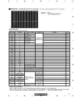
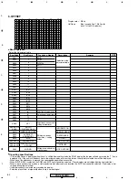
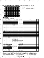
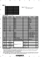
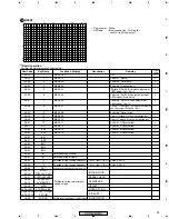
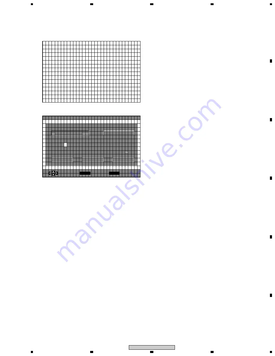
16. MEMO: Memo data are displayed and edited.
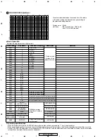
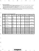
17. SERVICE PARTS : The PD number of the module microcomputer is rewritten to the parts recognition number for service.
See "7.1.3 AUTOMATIC BACKUP OF DIGITAL VIDEO ASSY DATA ".
Parts recognition number for service: Modify the leftmost digit of the PD number to F
Example: F691 (an original PD number is 5691).
Note:
Modification of the PD number to the ID number for service is needed only for the EEPROM of the module microcomputer.
The ID number for service in the data area of the module microcomputer in the EEPROM of the main microcomputer must not be
changed.
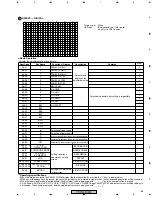
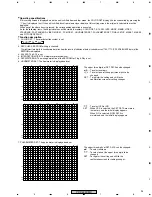
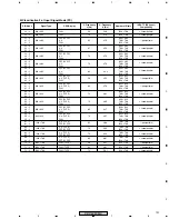
18. PICTURE DEFAULT
• The data adjusted in Service Factory mode will become the new default settings for PICTURE, WHITE BAL, and SIDE MASK LEVEL of the
Integrator menu.
• As long as PICTURE DEFAULT or FINAL SETUP is not executed, the settings made in Service Factory mode are not reflected in the video
output data in modes other than Service Factory mode.
• To make the values adjusted during Service Factory mode go into force, PICTURE DEFAULT must be executed after adjustment.
Note:
If PICTURE DEFAULT is executed:
<MEMO/SELECT>
• With the
5
or
∞
key, a MEMO to be edited can be selected.
• If you press the SET key, the screen shifts to MEMO/EDIT.
• If you select BACK and then press the SET key, the screen
shifts to the next higher layer.
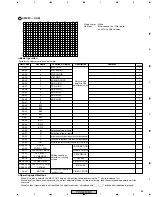
<MEMO/EDIT>
• For details on editing, see "INPUT Label" of the user menu.
• The default display is "_ _ _ _ _ _ _ _ _ _ _ _".
• When RESET is selected, the setting is reset to the default.
1
All the PICTURE items set on the user menu are reset.
2
The values for PICTURE, WHITE BAL, and SIDE MASK LEVEL of the Integrator menu will become those of current adjustment values of
Service Factory mode.
I N I T
M E M O
B A C K
–
– – – – – – – – – – –
– – – – – – – – – – –
– – – – – – – – – – –
– – – – – – – – – – –
–
–
–
–
–
S 1
I N 4 – 0 2 –
∗
2
N T
# 1
M E M O
P
P
D
- 5 0 3
B
A
R E S E T
S P A C E
E N D
B
C
D
E
F
G
H
I
J
K
L
M
N
O
Q
R
S
T
U
V
W
X
Y
Z
0
1
2
3
4
5
6
7
8
9
.
,
`
'
/
-
(
)
@
∗
:
#
?
&
ACK
SPACE
M X
P
SET
E
M NU
SET
SEL ECT
EX I T
1
5
10
15
16
1
5
10
15
20
25
30
32
1
5
10
15
16
1
5
10
15
20
25
30
32
Содержание PDP 433CMX
Страница 14: ...14 PDP 433CMX Upper side 8 9 1 Upper side Upper side 9 7 5 6 2 10 10 8 8 2 5 UNDER LAYER SECTION 4 ...
Страница 26: ...26 PDP 433CMX 2 13 UPPER LAYER SECTION 2 10 10 12 SW101 100V 200V P4 P7 P3 P5 P6 P2 P1 VM1 6 7 4 8 5 1 9 3 ...
Страница 165: ...165 PDP 433CMX Pin Assignment Top View CXA3516R RGB ASSY IC4603 AD PLL IC ...
Страница 166: ...166 PDP 433CMX Block Diagram ...
Страница 167: ...167 PDP 433CMX Pin Function ...
Страница 168: ...168 PDP 433CMX ...
Страница 169: ...169 PDP 433CMX ...

