133
PDP-433CMX
5
6
7
8
5
6
7
8
C
D
F
A
B
E
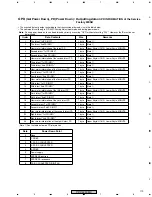
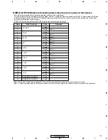
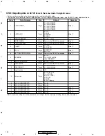
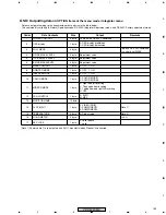
Number
of
Blinks
P.D. Point in
Operation
Error Point
Possible Part in failure
Circuit State
P.D. Circuit
in Operation
Diagnosis Condition
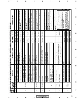
1
Y
DRIVE
IC22
0
6, IC22
14
(Pulse module), IC22
03, IC22
0
4
,
IC22
12, IC22
13, IC22
16, IC22
17, R22
0
9
K22
11
Lo
VCP OCP
2
Y
DC DC
VOFS D/D CONV. BLOCK (Y DRIVE Assy)
IC2
7
02, IC2
7
0
9, IC2
7
15
K
2
7
12
Lo
VOFS OVP
VOFS D/D CONV. BLOCK (Y DRIVE Assy)
IC2
7
0
1,
IC2
7
02, IC2
7
0
9, IC2
7
15
K
2709
L
o
VOFS UVP
Drive section (control signals, output elements etc.)
in normal operation
Q22
11
, Q22
12, R22
7
7, IC22
0
8, IC22
10
VOFS D/D CONV. BLOCK in normal operation
VH D/D CONV. BLOCK (Y DRIVE Assy)
IC2
7
12, IC2
7
16
K
2
7
19
Lo
VH OVP
VH D/D CONV. BLOCK (Y DRIVE Assy)
IC2
7
11
, IC2
7
12, IC2
7
16
K2
7
18 Lo
VH UVP
Drive section (control signals, output elements etc.)
in normal operation
SCAN (A), (B) Assy
SCAN IC
VH D/D CONV. BLOCK in normal operation
IC
5V D/D CONV. BLOCK (Y DRIVE Assy)
IC2
7
0
4, IC2
7
0
6, IC2
7
17
SCAN Assy in normal operation
SCAN (A), (B) Assy
Y DRIVE Assy
SCAN IC
K2
7
13 Lo
IC
5V UVP
IC
5V D/D CONV. BLOCK in normal operation
IC
5V D/D CONV. BLOCK (Y DRIVE Assy)
IC2
7
0
4, IC2
7
0
6, IC2
7
17
SCAN Assy in normal operation
3
X
DC DC
VRN D/D CONV. BLOCK (X DRIVE Assy)
IC3
7
02, IC3
7
12
K
3708
L
o
VRN OVP
VRN D/D CONV. BLOCK (X DRIVE Assy)
IC3
7
0
1,
IC3
7
02, IC3
7
12
K
3705
L
o
VRN UVP
Drive section (control signals, output elements etc.)
in normal operation
X DRIVE Assy
Q3
12
2
VRN D/D CONV. BLOCK in normal operation
4
X
DRIVE
X DRIVE Assy
IC32
0
0, IC32
0
1 (pulse module), IC3
103, IC3
10
4,
IC3
10
6, IC3
10
7, IC3
11
0, IC3
11
3, R3
10
9
K3
103 Lo
VCP OCP
5
PS
X DRIVE Assy
IC32
0
0, IC32
0
1 (Pulse module)
In a case where PD does not occur if the P4 connector is
disconnected
Y DRIVE Assy
IC22
0
6, IC22
14
(Pulse module)
In a case where PD does not occur if the P3 connector is
disconnected
MX AUDIO Assy
IC
8
6
0
1 (Audio IC)
In a case where PD does not occur if the P6 connector is
disconnected
In a case where PD does not occur if Pin 5 of the P2
connector is disconnected
SW POWER SUPPLY Module
SW POWER SUPPLY Module
In a case where the voltage is not output even if the P4, P3,
P6 connectors and Pin 5 of the P2 connectors are
disconnected
6
ADR
ADDRESS CONNECT A~D Assy
ADDRESS CONNECT A - D Assy,
RESONANCE Assy,
D/D CONV. BLOCK (DIGITAL VIDEO Assy)
Disconnection of the D8 - D15 connectors
7
ADR K
RESONANCE Assy
TCP damage of IC6704 (ICP), disconnection of the
D16 and D17 connectors, panel microcomputer is
defective, external Flash ROM of the panel
microcomputer is defective.
8
DIGITAL
DC DC
D/D CONV. BLOCK (DIGITAL VIDEO Assy)
IC1901
K1
9
0
1 L
o
5.
0V OVP
ADR. PD
ADR. K. PD
K
19
02 Lo
5.
0V UVP
D/D CONV. BLOCK (DIGITAL VIDEO Assy)
IC1901
K
19
03 Lo
3.3V OVP
K
19
0
4
Lo
3.3V UVP
D/D CONV. BLOCK (DIGITAL VIDEO Assy)
IC1901
K
19
0
5
Lo
2.
5V OVP
K
19
0
6
Lo
2.
5V UVP
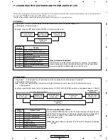
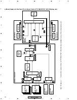
Diagnosis of error points in the various protection-circuit (P.D. circuits) operations (Red "STANDBY/ON" LED blinks)
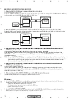
Note on PS PD
The condition that Red "STANDBY/ON" LED
blinks five times (power supply PD)
1
When the internal protection circuit of the
SW POWER SUPPLY Module worked
2
When a microcomputer was not able to
identify the PD point
↓
Care must be taken because five blinks of
the red LED does not always mean that the
protection circuit of the SW POWER SUPPLY
Module is activated.
Содержание PDP 433CMX
Страница 14: ...14 PDP 433CMX Upper side 8 9 1 Upper side Upper side 9 7 5 6 2 10 10 8 8 2 5 UNDER LAYER SECTION 4 ...
Страница 26: ...26 PDP 433CMX 2 13 UPPER LAYER SECTION 2 10 10 12 SW101 100V 200V P4 P7 P3 P5 P6 P2 P1 VM1 6 7 4 8 5 1 9 3 ...
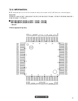
Страница 165: ...165 PDP 433CMX Pin Assignment Top View CXA3516R RGB ASSY IC4603 AD PLL IC ...
Страница 166: ...166 PDP 433CMX Block Diagram ...
Страница 167: ...167 PDP 433CMX Pin Function ...
Страница 168: ...168 PDP 433CMX ...
Страница 169: ...169 PDP 433CMX ...

