93
PDP-433CMX
5
6
7
8
5
6
7
8
C
D
F
A
B
E
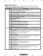
: To select YES or NO
SET
: When YES is selected, the SET DATA are stored
in memory, and the initial display appears.
When NO is selected, NOW DATA is
maintained, and the initial display appears.
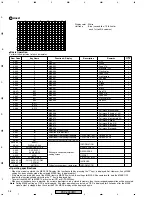
• If this setting screen is displayed when the unit is shifted from another mode, the COLOR DET display (the function called by pressing the
"1" key) is displayed first. If the unit is shifted back from a lower-layer display of this setting screen, the originally selected item will be
displayed.
• When any of the above keys is pressed, the corresponding operation is executed.
• As for the following items, the adjusted values will be stored in memory: COLOR DET., ACL SW, INTE. MODE, MEMO, VIDEO
STANDARD, PC STANDARD, VIDEO MODE 1, PC MODE 1, HOURMETER SET, PULSEMETER SET, FINAL SETUP, MASK 1, MASK 2,
and PICTURE DEFAULT.
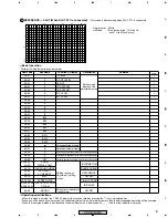
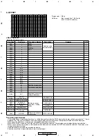
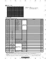
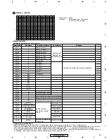
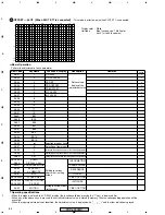
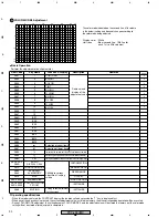
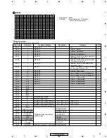
1. COLOR DET. : The color detection system is set.
2. EEP CHECK: EEPROM writing is checked.
The rightmost two digits in hexadecimal notation from the results of addition of data at subaddresses 1760-177C (PDC XGA/SHARP data) of the
EEPROM are displayed.
3. ACL SW: The ACL is set.
4. INTEGRATOR MODE: The integrator protection is set.
5. P&P WRITE ENA: The writing permission of the EEPROM for Plug & Play is set.
6. HOURMETER SET: The hourmeter is displayed and set.
7. PULSEMETER SET: The pulse meter is displayed and set.
EURO
SA
ALL
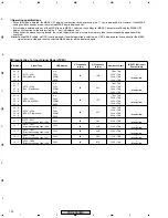
Operating specifications
Function description
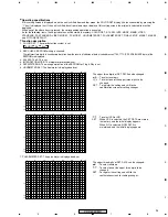
The upper three digits of SET DATA can be changed:
5∞
: To select numbers
: To select one of the upper three digits to be
changed
SET : To register the setting and shift to the
confirmation screen for setting changes.
The upper three digits of SET DATA can be changed:
5∞
: To select numbers
: To select one of the upper three digits to be
changed
SET : To register the setting and shift to the
confirmation screen for setting changes.
I N I T
H
N OW
D A T A : 1 2 3 4 5 H
S E T
D A T A : 0 9 7 0 0 H
O U R
E
M
T E R
S E T
–
–
S 1
I N 4 – 0 2 –
∗
2
N T
# 1
I N I T
P
N OW
D A T A : 1 2 3 4 5
6
.
7 G
S E T
D A T A : 0 9 7 0 0
0
.
0 G
U L S
M
E
E T
R
E
S E T
–
–
S 1
I N 4 – 0 2 –
∗
2
N T
# 1
I N I T
H
N O
Y E S
O U R
E
M
T E R
S E T
?
–
–
S 1
I N 4 – 0 2 –
∗
2
N T
# 1
1
5
10
15
16
1
5
10
15
20
25
30
32
1
5
10
15
16
1
5
10
15
20
25
30
32
1
5
10
15
16
1
5
10
15
20
25
30
32
Содержание PDP 433CMX
Страница 14: ...14 PDP 433CMX Upper side 8 9 1 Upper side Upper side 9 7 5 6 2 10 10 8 8 2 5 UNDER LAYER SECTION 4 ...
Страница 26: ...26 PDP 433CMX 2 13 UPPER LAYER SECTION 2 10 10 12 SW101 100V 200V P4 P7 P3 P5 P6 P2 P1 VM1 6 7 4 8 5 1 9 3 ...
Страница 165: ...165 PDP 433CMX Pin Assignment Top View CXA3516R RGB ASSY IC4603 AD PLL IC ...
Страница 166: ...166 PDP 433CMX Block Diagram ...
Страница 167: ...167 PDP 433CMX Pin Function ...
Страница 168: ...168 PDP 433CMX ...
Страница 169: ...169 PDP 433CMX ...


