100
PDP-433CMX
1
2
3
4
C
D
F
A
B
E
1
2
3
4
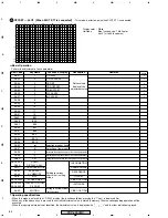
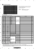
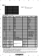
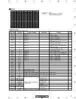
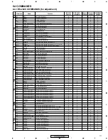
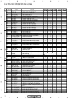
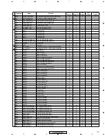
SIG Mode
Signal Type
OSD display
V. Frequency
fv (Hz)
H. Frequency
fh (Hz)
Number of Pixels
INPUT5 (DVI input)
Compatibility
00 • 6
00 • 7
00 • 8
00 • 9
SDTV • 625i
(PAL/SECAM)
4 : 3
FULL
ZOOM
WIDE
50
15.6
784
×
768
1024
×
768
1024
×
768
1024
×
768
×
(incompatible)
01 • 6
01 • 7
01 • 8
01 • 9
SDTV • 625p
(PAL • Progressive)
4 : 3
FULL
ZOOM
WIDE
50
31.2
784
×
768
1024
×
768
1024
×
768
1024
×
768
×
(incompatible)
02 • 6
02 • 7
02 • 8
02 • 9
SDTV • 525i
(NTSC/4.43NTSC)
4 : 3
FULL
ZOOM
WIDE
60
15.7
784
×
768
1024
×
768
1024
×
768
1024
×
768
×
(incompatible)
03 • 6
03 • 7
03 • 8
03 • 9
SDTV • 525p
(NTSC • Progressive)
4 : 3
FULL
ZOOM
WIDE
60
31.5
784
×
768
1024
×
768
1024
×
768
1024
×
768
×
(incompatible)
11 • 7
HDTV • 1125i
(Effective scanning lines: 1080)
FULL
50
28.1
1024
×
768
×
(incompatible)
12 • 7
HDTV • 1125i
(Effective scanning lines: 1080)
FULL
60
33.8
1024
×
768
×
(incompatible)
13 • 7
HDTV • 1125i
(Effective scanning lines: 1035)
FULL
60
33.8
1024
×
768
×
(incompatible)
14 • 7
HDTV • 750p
(Effective scanning lines: 720)
FULL
60
45.0
1024
×
768
×
(incompatible)
15 • 7
HDTV • 1125p
(Effective scanning lines: 1080)
FULL
60
67.5
1024
×
768
×
(incompatible)
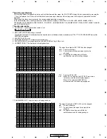
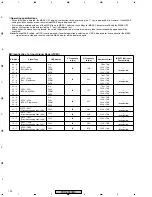
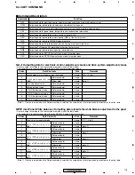
Classification 1 of Input Signal Mode (VIDEO)
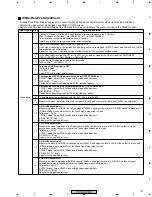
• When this mode is entered, the MASK OFF display (the function called by pressing the "1" key) is displayed first. However, if any MASK
setting has been already made, the selected MASK item is displayed first.
• If this mode is entered with any of the MASK items in MASK 1 selected, the settings for MASK 1 become invalid, and the MASK OFF
display (the function called by pressing the "1" key) is displayed first.
• When any of the above keys is pressed, the current adjustment value is stored in memory, then the corresponding operation will be
executed.
Note:
During MASK setting, an OSD is not displayed. If another operation is selected, an OSD is displayed for 2 seconds after the MASK
signal output is stopped, then the selected MASK display will be displayed again.
Operating specifications
Содержание PDP 433CMX
Страница 14: ...14 PDP 433CMX Upper side 8 9 1 Upper side Upper side 9 7 5 6 2 10 10 8 8 2 5 UNDER LAYER SECTION 4 ...
Страница 26: ...26 PDP 433CMX 2 13 UPPER LAYER SECTION 2 10 10 12 SW101 100V 200V P4 P7 P3 P5 P6 P2 P1 VM1 6 7 4 8 5 1 9 3 ...
Страница 165: ...165 PDP 433CMX Pin Assignment Top View CXA3516R RGB ASSY IC4603 AD PLL IC ...
Страница 166: ...166 PDP 433CMX Block Diagram ...
Страница 167: ...167 PDP 433CMX Pin Function ...
Страница 168: ...168 PDP 433CMX ...
Страница 169: ...169 PDP 433CMX ...

