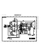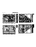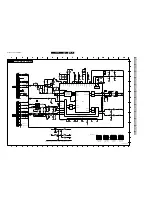
Circuit description new circuits
GB 51
L9.2E
9.
9.6
Video Signal Processing (see circuit diagram
A6)
9.6.1
Introduction:
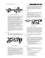
The video signal processing can be divided in the following
parts:
•
CVBS/Y/C input selection
•
Luminance and chrominance signal processing
•
PAL and SECAM demodulation /Auto system manager
•
YUV/RGB processing/ black stretcher
•
Second RGB insertion
•
RGB processing
•
Black current calibration loop
•
Beaming current limiting
Above mentioned processing circuits are integrated in the TV-
processor (parts B and C). The surrounding components are
for the adaptation of the selected application. The I2C bus is
used for defining and controlling the signals.
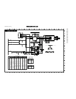
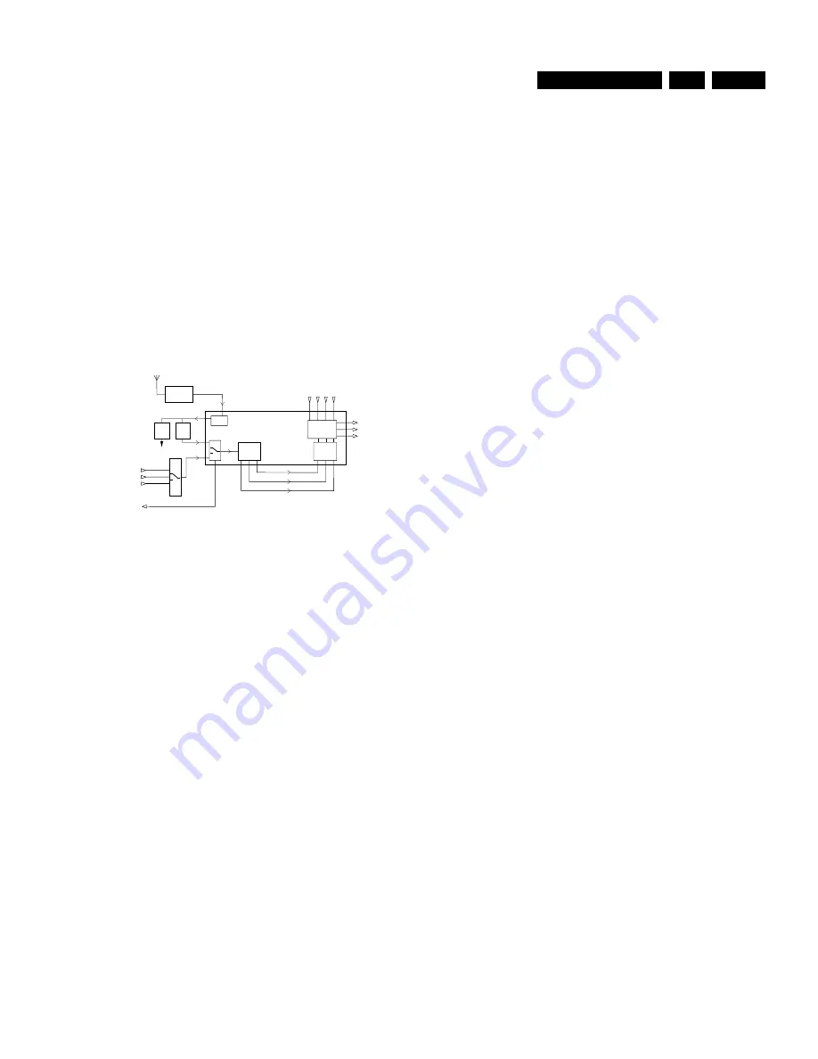
Figure 9-15 “Videopath”
9.6.2
CVBS/Y/C selection
The input switches are used for selection of the input signal.
Three input signals can be selected:
•
Pin 13: terrestrial CVBS input.
•
Pin 17: external AV1 input.
•
Pin10/11: external AV2-Y, CVBS/C input
When pin 11 is in the CVBS input mode then pin 10 is not used.
When pin 11 is in the Y/C input mode then both pins are used
and the CHROMA filter in the Y signal path is switched off.
9.6.3
Luminance / Chroma signal processing
Once the signal source has been selected, CHROMA filter
calibration is performed. The received colour burst-sub-carrier
frequency is used for the calibration. Correspondingly, the
CHROMA band-pass filter for PAL processing or the cloche
filter for SECAM processing is switched on. Pins 34, 35 have
the crystals connected to them. These crystals are used for
multi-purpose calibration of the burst sub-carrier. The selected
luminance signal is then supplied to the Horizontal and Vertical
synchronisation processing circuits and to the luminance
processing circuits. In the Luminance processing block, the
luminance signal is applied to the CHROMA trap. This trap is
switched on or off depending upon on the colour burst
detection of the CHROMA calibration circuit. Before the
luminance signal is applied to pin 28 of the TV-processor the
signal is applied to a "peaking" and "coring" circuit. In these
circuits the sharpness and noise level of the signal can be
influenced via the remote control (control menu in the user
menu ).
9.6.4
PAL and SECAM demodulation via the Auto system
manager
The colour decoder circuit detects whether the signal is a PAL
signal. The result is made known to the auto system manager.
The base-band delay line is activated when a PAL or SECAM
signal is detected. For the SECAM colour standard a reference
voltage is generated at pin16 of the TV-processor.
Connected at Pin 9 of the TV-processor, is the band-gap de-
coupling circuit, which consists of (2214,2215). The band-gap
circuit provides a very stable and temperature independent
reference voltage. It ensures optimal performance of the TV-
processor and is used by almost all functional blocks inside the
processor. The Y signal and the demodulator outputs R-Y and
B-Y are present at pin 28, 29, 30 of the TV-processor. The auto
system manager identifies PAL and SECAM colour standards
and is controllable via the IIC bus. Connected on pin 36 of the
TV-processor is the Loop Filter for the phase detector The filter
chosen provides an optimal transient response, which ensures
both an optimum for noise bandwidth and colour acquisition
time.
9.6.5
YUV / RGB processing/ black stretching
The signal Y, R-Y and B-Y present on pins 27, 31, 32 of the TV-
processor are used as the input signals for the colour decoding
section of the BiMOS (IC7520-C). The YUV processor enables
the colour saturation control and also converts the Y, B-Y and
B-Y signals to the R, G, B signal format via the colour matrix
circuit. The black stretcher circuit , initial stage of the matrix
circuit, extends the Grey signal level towards the actual black
level. The amount of extension depends upon the difference
between actual black level and the darkest part of the incoming
video signal level. This feature is fully integrated. The user can
switch this circuit on or off by using the Contrast Plus option in
the user menu.
9.6.6
Second RGB insertion
Pins 23, 24, 25 are used as the inputs for the second R, G, B
signals insertion. Pin 26 of the TV-processor is the input for the
insertion control signal which is called "FBL". When the FBL
signal level becomes higher than 0.9V (but less than 3V) the R,
G, B signals at pins 23,24,25 are inserted into the picture by
using the internal switches incorporated in the TV-processor.
This second insertion possibility is used for insertion of the on
screen display signals , TXT or R. G. B signals from the SCART
socket.
9.6.7
RGB processing
The RGB processing circuit enables the picture parameters to
be adjusted by using a combination of the user menus and the
remote control. Additionally automatic gain control for the RGB
signals via cut-off stabilisation is achieved in this functional
block..
The block also inserts the cut off point "measuring pulses" into
the RGB signals during vertical retrace period.. From outputs
19,20 and 21 the RGB signals are then applied to the output
amplifiers on the CRT panel.
9.6.8
Black current calibration loop
The black current calibration loop ensures that the white
balance at low signal levels and low light white balance is
skipped. By means of the inserted measuring pulses, the black
current calibration loop, tracks the beam current feed back of
the RGB signals at the cathodes of the picture tube. As a result
of this calibration, the individual black level of the RGB output
signals is shifted to a level which allocates around 10uAof
beam current to each of the RGB signals. Pin 18 (BC_info) of
YC/CVBS EXT
YC/CVBS EXT
CVBS + SIF
R
G
B
TDA884X
SWITCH
V_PATH1.PPT
20/3/98
TUNER
SOUND
TRAP
IF
CVBS_INT
SOUND
BPF
SIF
(to sound proc..)
CVBS_EXT
CVBS_MON
IF
48/49
25
21
32
38
6
13
17
30
29
28
27
31
19
20
24
23
26
CHROMA
PROCESSING
MATRIX
RGB
PROCESSING
+ SWITCH
YC/CVBS EXT
R
G
B
FBL
OSD/TXT/SCART
TO CRT
Y
U
V
CL 86532104_017.eps
160299
TDA 8844/8845
Содержание L9.2EAA
Страница 5: ...Directions for use GB 5 L9 2E 3 3 Directions for use ...
Страница 6: ...Directions for use GB 6 L9 2E 3 ...
Страница 7: ...Directions for use GB 7 L9 2E 3 ...
Страница 31: ...Schematics and PWB s GB 31 L9 2E 7 ...
Страница 32: ...Schematics and PWB s GB 32 L9 2E 7 ...
Страница 38: ...Schematics and PWB s GB 38 L9 2E 7 ...
Страница 42: ...Schematics and PWB s GB 42 L9 2E 7 Personal notes Personal notes ...

