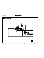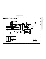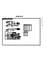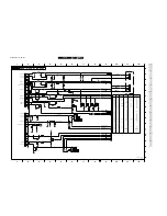
Circuit description new circuits
GB 47
L9.2E
9.
9.
Circuit description new circuits
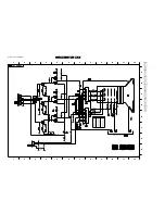
Power supply (diagram A1)
9.1
Introduction
9.1.1
General
The switch mode power supply (Fixed Frequency ) is mains
isolated. The control IC7520 (MC44603A) produces pulses for
driving FET 7518. Power supply regulation is achieved by
using duty cycle control at a fixed frequency of nominal 70 kHz
in normal operation. In stand-by, slow-start and overload
situations the SMPS runs at frequencies other than 70 kHz.
Basic characteristics of this SMPS :
•
Mains Isolated flyback Converter type
•
Input range : 150 - 276 Volts AC
•
Secundaire voltage adjustment via potentiometer R3540 at
the primary side
•
IC7520 is featured with Slow-Start circuitry
•
Protection Circuits
•
Degaussing circuit
9.1.2
Output voltages
•
AudioSupply 10V/14V ( +18V ) for the Sound amplifier ( D2
)
•
Vbatt/MainSupply ( +95V ) for the Line deflection stage
(A2), Tuner video IF ( A5 )
•
Vaux / MainAux ( +9.5V ) for the Line Deflection ( A2 ) and
the Control (A7)
9.1.3
The switching periods of TS7518
The power supply duty cycle is dependent on the T-on of FET
7518. The FET is driven by pin 3 of IC7520. This IC controls the
secondary voltage (VBATT via potentiometer 3540. The
primary voltage at pin1-2 of transformer 5545 is rectified by
D6537 and smoothed by C2537. The switching period of
TS7518 can be divided into three main phases: Duty cycle T-
on, T-off and T-dead.
•
During T-on, FET 7518 conducts.
•
Energy is stored in the primary winding (4-7) of transformer
T5545 by using a linear increasing primary current. The
slope depends on the rectified mains-voltage present
across C2508. The T-on period is varied to provide
regulation of the drive waveform at pin 3 of IC7520. By
controlling the duty cycle of the SMPS in this way the
(VBATT is controlled.
•
During T-off, FET 7518 is switched off and therefore does
not conduct. The energy is now transferred to the
secondary side of the transformer and then supplied to the
load via the secondary diodes (D6550, D6560 and D6570).
The current through the secondary side of the transformer
decreases until it reaches zero.
•
During T-dead FET 7518 does not conduct .The voltage at
the drain of the FET decays and eventually reaches the
input voltage of approximately 300V.
9.2
Primary side
9.2.1
Mains input and degaussing
•
Mains voltage: this voltage is filtered by L5500 and L5501,
rectified by the bridge diode 6502 .. 6505 and then
smoothed by C2508 which provides a DC input voltage of
300V DC for an ac input voltage of 230V.
•
Degaussing : R3504 is a PTC. When switching "on" the set,
the PTC is cold and has a low-ohmic value. This allows a
very high degaussing current at initial power on. The PTC
will then heat up due to the high current involved and
becomes high-ohmic which reduces the degaussing-
current. During normal operation, the degaussing current is
signal.very small, because of the high impedance of PTC
R3504.
9.2.2
Start up and take over
•
Start-up : The start-up circuitry consisting of 3510, 3530
and 3529 use the voltage coming from the 230V AC mains
to start-up IC7520 via the supply pin 1. The output drive
waveform (pin 3) is blocked by using the ICs internal logic
until the voltage on pin 1 reaches 14.5 Volts however with
less than 14.5 volts on Pin 1 the IC only consumes 0.3mA.
Once pin 1 reaches the 14.5 Volts threshold, IC7520 will
start up (FET 7518 will conduct) and pin 1 sinks a typical
supply current of about 17 mA. This supply current cannot
be delivered by the start-up circuitry, so a take-over circuit
must be present. If take-over does not occur then the
voltage on pin 1 will decrease below 9V and IC7520 will
switch off. The supply begins a new Start-up cycle, see top
of this paragraph. This cycle will repeat itself and can be
noticed by an audible hick-up sounding noise.
•
Take over : During start-up a voltage across winding 1-2 is
gradually built up. At the moment the voltage across
winding 1-2 reaches approx. (14.5 Volts, D6540 start
conducting and takes over the supply voltage Vpin 1 of
IC7520 (take over current is approx. 17mA).
Note: This power supply is a FFS (= Fixed Frequency Supply)
and not a SOPS (= Self Oscillating Power Supply).
9.3
Control circuitry
9.3.1
IC7520 control mechanisms
IC7520 controls the T-on time of FET 7518 in three different
ways:
•
"Primary-voltage-sensing" controls the secondary output
voltages via the feedback voltage pin 14
•
"Primary current sensing" controls the maximum primary
current via the current sense voltage pin 7
•
"Demagnetization control" prevents the transformer T5545
from going into saturation via the so-called "DEMAG"
function at pin 8
9.3.2
Secondary voltage sensing (pin 14 of IC7520)
When the output vVBATT increases (due to a reduction
in the load ) the primary voltage at winding 1-2 will increase,
therefore the voltage across capacitor 2537 increases. This will
reduce the on-time of FET 7518 due to an increase of the
voltage present on pin 14.
In the event of an increase of the load (decrease of output
vVBATT ), the control circuit will work in the opposite
way to the explanation above.
9.3.3
Primary sensing (pin 7 of IC7520)
The current sense voltage at pin 7 is used to measure the
primary current through FET7518. The primary current is
converted into a voltage by R3518.
Содержание L9.2EAA
Страница 5: ...Directions for use GB 5 L9 2E 3 3 Directions for use ...
Страница 6: ...Directions for use GB 6 L9 2E 3 ...
Страница 7: ...Directions for use GB 7 L9 2E 3 ...
Страница 31: ...Schematics and PWB s GB 31 L9 2E 7 ...
Страница 32: ...Schematics and PWB s GB 32 L9 2E 7 ...
Страница 38: ...Schematics and PWB s GB 38 L9 2E 7 ...
Страница 42: ...Schematics and PWB s GB 42 L9 2E 7 Personal notes Personal notes ...

